Scaling High-Performance TFP-TT-TPA Organic Semiconductors for Stable OFET Applications
Scaling High-Performance TFP-TT-TPA Organic Semiconductors for Stable OFET Applications
The rapid evolution of flexible electronics and transparent displays demands organic semiconductor materials that not only exhibit high carrier mobility but also possess exceptional environmental stability, particularly against light irradiation. Patent CN115124547A introduces a groundbreaking solution with the synthesis of 4,4'-(3,6-bis(3,4,5-trifluorophenyl)thieno[3,2-b]thiophene-2,5-diyl)bis(N,N-diphenylaniline), commonly referred to as TFP-TT-TPA. This small-molecule organic semiconductor addresses the critical industry pain point of photo-instability, where traditional materials suffer from significant photocurrent increases and threshold voltage shifts under operation. By leveraging a sophisticated Donor-Acceptor (D-A) molecular architecture, this material achieves intrinsic light insensitivity, making it a prime candidate for next-generation optoelectronic devices that must operate reliably under ambient or even intense lighting conditions exceeding 100mW/cm².
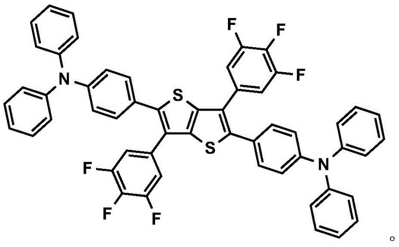
For R&D directors and procurement specialists in the electronic chemicals sector, the commercial viability of TFP-TT-TPA lies in its robust synthetic pathway which utilizes widely available starting materials and standard catalytic processes. The molecular design strategically incorporates trifluorophenyl groups as strong electron-withdrawing units and triphenylamine moieties as potent electron-donating groups on a thienothiophene core. This specific arrangement facilitates efficient intramolecular charge transfer while simultaneously quenching photogenerated excitons that typically degrade device performance. As a reliable organic semiconductor material supplier, understanding the nuances of this synthesis allows for better quality control and cost management in the production of high-purity OLED material and OFET components.
The Limitations of Conventional Methods vs. The Novel Approach
The Limitations of Conventional Methods
Historically, the development of organic field-effect transistors (OFETs) has been hindered by the inherent instability of many small-molecule semiconductors when exposed to external stimuli, particularly light. Conventional materials often lack the structural rigidity or electronic configuration necessary to resist photo-oxidation or trap formation under illumination. In standard operating environments, these materials frequently exhibit a dramatic increase in off-current and a substantial drift in threshold voltage, rendering them unsuitable for applications requiring long-term stability, such as flexible transparent displays or sensors operating in variable lighting. Furthermore, traditional synthesis routes for high-mobility semiconductors often involve complex multi-step procedures with low overall yields and difficult purification requirements, leading to batch-to-batch variability that complicates commercial scale-up of complex polymer additives and small molecules alike.
The Novel Approach
The novel approach detailed in the patent overcomes these limitations through a rational molecular design that integrates photostability directly into the chemical structure. By constructing a centrosymmetric D-A system, the material effectively manages excited states, preventing the accumulation of charges that lead to device degradation. Experimental data confirms that OFETs fabricated with this material maintain stable transfer characteristic curves even under strong light irradiation with power densities surpassing sunlight intensity. This represents a significant leap forward in cost reduction in electronic chemical manufacturing, as it reduces the need for expensive encapsulation layers or complex device architectures solely designed to block light. The synthesis method is streamlined into three main stages, utilizing Suzuki-Miyaura cross-coupling reactions which are well-understood and scalable in industrial settings.
Moreover, the device fabrication process supports both thermal evaporation for thin films and physical vapor transport for micro-nanocrystals, offering flexibility in manufacturing methods. The resulting devices show negligible changes in photocurrent and threshold voltage across a wide range of light intensities, validating the material's superior photostability. For supply chain heads, this reliability translates to reduced failure rates in end-products and a more predictable performance profile, essential for reducing lead time for high-purity electronic chemicals in competitive markets.
Mechanistic Insights into Suzuki-Miyaura Cross-Coupling and D-A Architecture
The synthesis of TFP-TT-TPA relies heavily on the precision of palladium-catalyzed Suzuki-Miyaura cross-coupling reactions, which allow for the precise assembly of the conjugated backbone. The first critical step involves the coupling of 3,6-dibromothieno[3,2-b]thiophene with 3,4,5-trifluorophenylboronic acid. This reaction establishes the electron-deficient core of the molecule. The presence of three fluorine atoms on the phenyl ring significantly lowers the LUMO energy level, enhancing the electron-accepting capability of this segment. The reaction conditions specified, utilizing tetrakis(triphenylphosphine)palladium as the catalyst and potassium carbonate as the base in a toluene/ethanol/water solvent system, are optimized to ensure complete conversion while minimizing homocoupling side products that could act as charge traps.
Following the initial coupling, the intermediate undergoes selective bromination using N-bromosuccinimide (NBS). This step is crucial for activating the 2,5-positions of the thienothiophene core for the subsequent attachment of the electron-donating groups. The use of glacial acetic acid and chloroform as solvents ensures controlled reactivity, preventing over-bromination which would lead to structural defects. The final coupling with (4-(diphenylamino)phenyl)boronic acid introduces the bulky triphenylamine units. These groups not only serve as electron donors to complete the D-A structure but also improve the solubility and film-forming properties of the final material. The steric bulk of the triphenylamine helps prevent excessive aggregation that might lead to excimer formation, further contributing to the material's photostability.

Impurity control is managed through rigorous purification protocols described in the patent. After each reaction step, the crude products are subjected to column chromatography using specific eluent ratios, such as ethyl acetate and petroleum ether, to separate the desired product from catalyst residues and unreacted starting materials. The final recrystallization steps, using solvents like ethyl acetate or chloroform at elevated temperatures, are essential for achieving the high crystallinity required for efficient charge transport. This attention to detail in purification ensures that the final semiconductor material meets the stringent purity specifications demanded by the semiconductor industry, minimizing defect densities in the active layer of the transistor.
How to Synthesize TFP-TT-TPA Efficiently
The synthesis of this advanced organic semiconductor requires strict adherence to inert atmosphere conditions and precise stoichiometric control to maximize yield and purity. The process is divided into three distinct chemical transformations, each building upon the previous intermediate to construct the final conjugated system. Operators must ensure that all solvents are anhydrous where specified and that oxygen is excluded to prevent catalyst deactivation. The following guide outlines the standardized procedure derived from the patent examples, providing a roadmap for laboratory scale-up and process optimization.
- Perform initial Suzuki coupling of 3,6-dibromothieno[3,2-b]thiophene with 3,4,5-trifluorophenylboronic acid using Pd(PPh3)4 catalyst.
- Execute selective bromination of the intermediate using N-bromosuccinimide (NBS) in glacial acetic acid and chloroform.
- Conduct final Suzuki coupling with (4-(diphenylamino)phenyl)boronic acid followed by rigorous column chromatography and recrystallization.
Commercial Advantages for Procurement and Supply Chain Teams
For procurement managers and supply chain strategists, the adoption of TFP-TT-TPA offers distinct advantages rooted in its synthetic efficiency and material performance. The reliance on Suzuki coupling means that the process utilizes commodity chemicals and widely available catalysts, avoiding the need for exotic or highly regulated reagents that often bottleneck production. This accessibility of raw materials significantly enhances supply chain reliability, ensuring that production schedules are not disrupted by sourcing difficulties. Furthermore, the robustness of the chemical structure implies a longer shelf life and easier handling compared to more sensitive organic semiconductors, reducing waste and inventory costs associated with material degradation.
- Cost Reduction in Manufacturing: The synthetic route avoids the use of expensive transition metal catalysts beyond standard palladium systems, and the purification steps utilize common solvent systems like petroleum ether and ethyl acetate. This simplifies the downstream processing and solvent recovery operations, leading to substantial cost savings in electronic chemical manufacturing. By eliminating the need for complex encapsulation technologies to protect against light degradation, device manufacturers can also reduce their Bill of Materials (BOM) costs, passing value down the supply chain.
- Enhanced Supply Chain Reliability: The starting materials, including 3,6-dibromothieno[3,2-b]thiophene and various boronic acids, are commercially available from multiple global suppliers, mitigating the risk of single-source dependency. The synthesis does not require cryogenic conditions or ultra-high vacuum during the chemical steps, allowing for production in standard fine chemical facilities. This flexibility enables diversified manufacturing locations, strengthening the resilience of the supply network against regional disruptions and ensuring consistent availability for high-volume applications.
- Scalability and Environmental Compliance: The reaction conditions, typically ranging from room temperature to 120°C, are energy-efficient and easily scalable from gram to kilogram quantities. The use of aqueous bases and recyclable organic solvents aligns with modern green chemistry principles, simplifying waste treatment and regulatory compliance. The ability to process the material via thermal evaporation or solution processing provides manufacturers with options to optimize their production lines for either high-throughput roll-to-roll coating or high-precision vacuum deposition, accommodating diverse market needs without retooling entire facilities.
Frequently Asked Questions (FAQ)
The following questions address common technical and commercial inquiries regarding the production and application of TFP-TT-TPA. These insights are derived directly from the experimental data and structural analysis provided in the patent documentation, offering clarity on performance metrics and processing parameters. Understanding these details is crucial for integrating this material into existing manufacturing workflows and ensuring optimal device performance.
Q: What makes TFP-TT-TPA superior for light-stable OFETs?
A: The molecule features a centrosymmetric Donor-Acceptor (D-A) structure where strong electron-withdrawing trifluorophenyl groups and electron-donating triphenylamine units quench photogenerated excitons, preventing threshold voltage drift under high light intensity.
Q: What are the critical purification steps for this semiconductor?
A: High purity is achieved through sequential column chromatography using ethyl acetate/petroleum ether mixtures and final recrystallization from ethyl acetate or chloroform, ensuring removal of palladium residues and unreacted boronic acids.
Q: Is this material suitable for large-scale thermal evaporation?
A: Yes, the material demonstrates excellent thermal stability and can be deposited as thin films (20-100nm) via thermal evaporation at substrate temperatures around 60°C, maintaining structural integrity and carrier mobility.
Partnering with NINGBO INNO PHARMCHEM: Your Reliable TFP-TT-TPA Supplier
As the demand for stable and high-performance organic semiconductors grows, partnering with an experienced CDMO becomes essential for success. NINGBO INNO PHARMCHEM possesses extensive experience scaling diverse pathways from 100 kgs to 100 MT/annual commercial production, ensuring that your supply needs are met with consistency and precision. Our state-of-the-art facilities are equipped with rigorous QC labs capable of verifying stringent purity specifications, including trace metal analysis and structural confirmation via NMR and MS, guaranteeing that every batch of TFP-TT-TPA meets the highest industry standards for electronic applications.
We invite you to collaborate with our technical team to explore how this photostable material can enhance your product lineup. Contact our technical procurement team today to request a Customized Cost-Saving Analysis tailored to your specific volume requirements. We are ready to provide specific COA data and route feasibility assessments to support your R&D and production planning, ensuring a seamless transition from laboratory innovation to commercial reality.