Advanced Synthesis of Dual-Emission Hexanuclear Cuprous Iodide Clusters for Next-Gen OLEDs
The landscape of organic light-emitting diode (OLED) materials is undergoing a significant transformation, driven by the urgent need for cost-effective, earth-abundant alternatives to precious metal complexes. Patent CN108586536B introduces a groundbreaking advancement in this sector with the development of a novel 2-[(2-dimethylaminophenyl)(phenyl)phosphine]-N,N-xylidine cuprous iodide complex. This hexanuclear cluster compound represents a strategic leap forward for reliable OLED material suppliers seeking to diversify their portfolio with high-performance luminescent materials. Unlike traditional mononuclear or binuclear copper complexes, this specific architecture leverages a unique chair-like Cu6I6 core wrapped by tridentate phosphine ligands, resulting in superior dual emission properties. The patent details a robust synthetic pathway that achieves a remarkable yield of 72%, demonstrating not only chemical elegance but also significant potential for cost reduction in electronic chemical manufacturing. By utilizing copper, an abundant and inexpensive transition metal, this technology addresses the critical supply chain vulnerabilities associated with iridium and platinum-based phosphors.
The Limitations of Conventional Methods vs. The Novel Approach
The Limitations of Conventional Methods
Historically, the development of efficient electroluminescent materials has been dominated by heavy metal complexes, particularly those based on iridium and platinum, which suffer from exorbitant costs and supply chain instability. While copper(I) complexes have emerged as a promising alternative, early iterations faced significant hurdles regarding stability and quantum efficiency. Mononuclear cuprous halide complexes, although exhibiting strong green emission and high quantum yields in solution, often struggle with structural instability in the solid state, leading to quenching effects that diminish device performance. Furthermore, many existing dinuclear or tetranuclear clusters require complex ligand systems that are difficult to synthesize on a large scale, often involving harsh reaction conditions or low-yielding purification steps. The reliance on specific, hard-to-source ligands creates bottlenecks for commercial scale-up of complex polymer additives and small molecule emitters alike, limiting their widespread adoption in mass-market display technologies.
The Novel Approach
The methodology outlined in CN108586536B circumvents these traditional limitations through the ingenious design of a hexanuclear cluster stabilized by a custom-synthesized tridentate ligand, 2-[(2-dimethylaminophenyl)(phenyl)phosphine]-N,N-xylidine (ppda). This approach facilitates the formation of a highly symmetric chair-like Cu6I6 core, which inherently possesses thermochromic and dual emission capabilities essential for high-quality white light generation. The synthesis strategy is remarkably streamlined, avoiding the need for exotic reagents or extreme temperatures during the final complexation step. As illustrated in the reaction scheme below, the process involves a straightforward substitution to create the precursor, followed by lithiation and phosphination to generate the ligand, and finally, a simple coordination reaction with cuprous iodide.
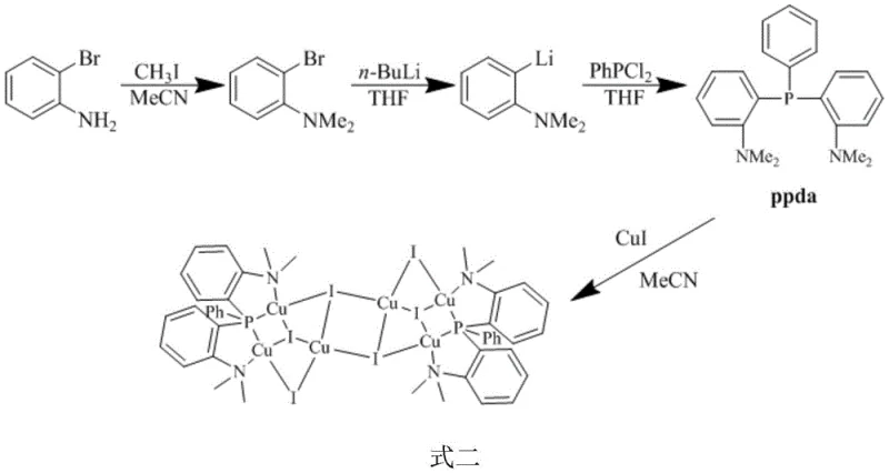
This streamlined workflow significantly lowers the barrier to entry for manufacturers, enabling high-purity OLED material production with reduced operational overhead. The ability to achieve a 72% yield using standard laboratory glassware and common solvents like dichloromethane underscores the practical viability of this method for industrial applications. Moreover, the resulting complex exhibits a solid-state quantum yield of 14.8% and emits white light, eliminating the need for multiple emissive layers in device fabrication, which further simplifies the downstream manufacturing process for display panels.
Mechanistic Insights into Hexanuclear Cluster Formation
The structural integrity and photophysical properties of the target product are deeply rooted in its unique coordination geometry. Crystallographic analysis reveals that the complex crystallizes in the monoclinic system with space group P2(1)/n, featuring a central Cu6I6 cluster where all copper atoms adopt a four-coordinate configuration. Specifically, four copper atoms exist in a CuPNI2 environment, while the remaining two reside in a CuI4 geometry, creating a distorted chair-like conformation that maximizes orbital overlap and stability. This specific arrangement is crucial for facilitating the Metal-to-Ligand Charge Transfer (MLCT) and Halide-to-Ligand Charge Transfer (XLCT) transitions observed in the UV-Vis absorption spectra. The bond lengths within the cluster, particularly the Cu-I bonds ranging from approximately 2.58 to 2.77 Angstroms, indicate strong covalent interactions that stabilize the cluster against dissociation under operational stress.
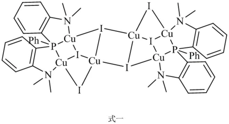
Furthermore, the presence of intermolecular hydrogen bonds and C-H...π interactions plays a pivotal role in defining the solid-state packing and, consequently, the emission characteristics. These weak non-covalent forces help to rigidify the molecular structure, suppressing non-radiative decay pathways that typically plague copper complexes at room temperature. The small energy gap (ΔE) between the singlet (S1) and triplet (T1) excited states allows for efficient reverse intersystem crossing (RISC), a hallmark of Thermally Activated Delayed Fluorescence (TADF). This mechanism ensures that both singlet and triplet excitons contribute to light emission, theoretically boosting internal quantum efficiency. For R&D teams, understanding these mechanistic nuances is vital for optimizing device architectures, as the balance between Local Excitation (LE) and Cluster Center (CC) emission can be tuned by modifying the ligand substituents without altering the core cluster topology.
How to Synthesize 2-[(2-Dimethylaminophenyl)(phenyl)phosphine]-N,N-xylidine Cuprous Iodide Complex Efficiently
The synthesis protocol described in the patent offers a reproducible pathway for generating this advanced luminescent material, suitable for both laboratory research and pilot-scale production. The process begins with the preparation of the ppda ligand via a multi-step sequence involving nucleophilic substitution and organolithium chemistry, followed by the final complexation with cuprous iodide. The simplicity of the final step, which proceeds at room temperature in dichloromethane, makes it particularly attractive for scaling. Detailed standardized synthesis steps are provided in the guide below to ensure consistency and purity.
- Synthesize the ppda ligand by reacting 2-bromoaniline with methyl iodide, followed by lithiation and reaction with dichlorophenylphosphine.
- Prepare the reaction mixture by combining the purified ppda ligand with cuprous iodide in a dry dichloromethane solvent under nitrogen.
- Stir the suspension at room temperature, filter the residue, and recrystallize from dichloromethane/acetonitrile to obtain the target white crystals.
Commercial Advantages for Procurement and Supply Chain Teams
For procurement managers and supply chain directors, the adoption of this copper-based technology presents a compelling value proposition centered on risk mitigation and cost optimization. The shift from precious metals to copper fundamentally alters the cost structure of OLED material production, removing exposure to the volatile pricing of rare earth elements. Additionally, the synthetic route utilizes commodity chemicals such as 2-bromoaniline, methyl iodide, and cuprous iodide, which are readily available from multiple global suppliers, ensuring supply continuity even during market disruptions. The elimination of expensive transition metal catalysts in the final step further reduces the burden on waste management and purification protocols, contributing to a leaner, more sustainable manufacturing operation.
- Cost Reduction in Manufacturing: The primary economic driver for this technology is the substitution of scarce precious metals with abundant copper, which drastically lowers the raw material cost per kilogram of the final emitter. The synthesis avoids the use of specialized high-pressure reactors or cryogenic equipment for the final complexation, allowing production to occur in standard stainless steel or glass-lined vessels. This compatibility with existing infrastructure means that manufacturers can integrate this new material line without significant capital expenditure on new hardware. Furthermore, the high yield of 72% minimizes material waste, directly improving the overall process mass intensity (PMI) and reducing the cost of goods sold (COGS) for the final electronic chemical product.
- Enhanced Supply Chain Reliability: Dependence on a single source for critical raw materials is a major vulnerability in the electronics supply chain. The precursors for this complex, including the phosphine ligands and copper salts, are produced by a wide network of chemical manufacturers globally, reducing the risk of supply bottlenecks. The robustness of the synthesis method, which tolerates standard laboratory conditions and does not require ultra-high purity inert atmospheres beyond standard nitrogen blanketing, simplifies logistics and storage requirements. This resilience ensures that reducing lead time for high-purity electronic chemicals becomes a achievable goal, allowing for faster response to market demand fluctuations in the display industry.
- Scalability and Environmental Compliance: The environmental footprint of this synthesis is significantly lower than traditional methods due to the absence of toxic heavy metals and the use of relatively benign solvents like dichloromethane and acetonitrile, which can be efficiently recovered and recycled. The solid-state stability of the final product reduces the need for specialized packaging or cold-chain logistics, simplifying distribution. From a regulatory perspective, copper-based materials generally face fewer restrictions regarding hazardous substance compliance (such as RoHS) compared to cadmium or lead-based alternatives, facilitating smoother market entry and certification processes for downstream device manufacturers seeking eco-friendly solutions.
Frequently Asked Questions (FAQ)
The following questions address common technical and commercial inquiries regarding the implementation of this hexanuclear cuprous iodide technology. These insights are derived directly from the patent specifications and are intended to clarify the operational benefits and performance metrics for potential partners and licensees.
Q: What are the luminescent properties of this hexanuclear cuprous complex?
A: The complex exhibits dual emission characteristics with a maximum emission wavelength at 474nm, producing white light in the solid state due to a small energy gap between S1 and T1 states, indicative of thermally activated delayed fluorescence (TADF).
Q: Why is the hexanuclear structure preferred over mononuclear complexes for OLEDs?
A: Polynuclear cuprous complexes, specifically the chair-like Cu6I6 core found in this patent, offer enhanced stability and unique cluster-centered (CC) emission modes that complement local excitation, resulting in broader spectrum white light emission compared to mononuclear variants.
Q: Is the synthesis method scalable for industrial production?
A: Yes, the synthesis operates at room temperature using common solvents like dichloromethane and acetonitrile, achieving a high yield of 72% without requiring expensive high-pressure equipment or cryogenic conditions beyond standard lithiation steps.
Partnering with NINGBO INNO PHARMCHEM: Your Reliable 2-[(2-Dimethylaminophenyl)(phenyl)phosphine]-N,N-xylidine Cuprous Iodide Complex Supplier
As the demand for next-generation display materials accelerates, partnering with an experienced CDMO is essential for translating patented innovations into commercial reality. NINGBO INNO PHARMCHEM possesses extensive experience scaling diverse pathways from 100 kgs to 100 MT/annual commercial production, ensuring that your supply needs are met with precision and consistency. Our state-of-the-art facilities are equipped with rigorous QC labs capable of verifying stringent purity specifications, guaranteeing that every batch of luminescent material meets the exacting standards required for high-performance OLED applications. We understand the critical nature of impurity profiles in electronic materials and employ advanced chromatographic techniques to ensure product integrity.
We invite you to collaborate with us to unlock the full potential of this copper-based luminescent technology. Our technical team is ready to provide a Customized Cost-Saving Analysis tailored to your specific production volumes and quality requirements. Please contact our technical procurement team today to request specific COA data and route feasibility assessments, and let us help you secure a competitive advantage in the rapidly evolving electronic materials market.