Advanced Fluorene Derivatives for High-Efficiency OLED Hole Transport Layers
Introduction to Next-Generation Hole Transport Materials
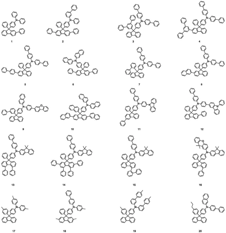
The rapid evolution of the organic light-emitting diode (OLED) industry demands materials that not only deliver high luminous efficiency but also ensure exceptional operational stability. Patent CN110724062A introduces a groundbreaking class of fluorene compounds specifically engineered to address the critical bottlenecks in hole transport layers (HTL). Unlike conventional materials that often suffer from thermal instability and rapid degradation under high current densities, these novel derivatives utilize a rigid spiro-fluorene backbone combined with bulky aryl substituents to enhance morphological stability. This structural innovation effectively balances hole mobility with electron blocking capabilities, preventing exciton quenching at the interface. As a reliable OLED material supplier, understanding the nuanced chemistry behind these structures is essential for developing next-generation displays that meet the rigorous standards of modern consumer electronics.
The Limitations of Conventional Methods vs. The Novel Approach
The Limitations of Conventional Methods
Traditional hole transport materials, such as N,N'-bis(naphthalen-1-yl)-N,N'-bis(phenyl)-benzidine (NPB), have long served as the industry standard but are increasingly showing their age in high-performance applications. The primary deficiency lies in their relatively low glass transition temperature, which leads to crystallization and morphological changes during device operation, drastically shortening the lifespan of the organic electroluminescent device. Furthermore, the HOMO energy levels of these conventional materials are not always optimally aligned with adjacent emissive layers, causing an imbalance in carrier injection that reduces overall quantum efficiency. In comparative studies, devices utilizing standard architectures often demonstrate T95 lifetimes of less than 80 hours at high brightness levels, which is insufficient for premium display applications requiring tens of thousands of hours of operation.
The Novel Approach
The patented technology circumvents these issues by introducing a sterically hindered fluorene core that physically prevents molecular packing and crystallization. By strategically substituting the fluorene scaffold with various aryl and heteroaryl groups, the synthesis creates a three-dimensional structure that maintains an amorphous state even under thermal stress. This approach not only enhances the thermal stability but also fine-tunes the electronic properties to match the energy levels of phosphorescent dopants. The result is a significant improvement in device performance, with experimental data showing lifetimes exceeding 160 hours under identical testing conditions, effectively doubling the operational durability compared to legacy materials. This represents a paradigm shift in how we approach the molecular design of electronic chemicals for the display sector.
Mechanistic Insights into Lewis Acid Catalyzed Coupling
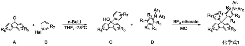
The synthetic strategy outlined in the patent relies on a robust two-step sequence that avoids the use of precious metal catalysts, which is a significant advantage for cost reduction in electronic chemical manufacturing. The first step involves the generation of a hydroxy-fluorene intermediate through the nucleophilic addition of an aryl-lithium species to a substituted fluorenone. This reaction requires precise temperature control, typically initiated at -78°C to manage the exothermic nature of the lithiation, followed by a gradual warm-up to room temperature to ensure complete conversion. The second, and perhaps most critical step, is the coupling of this alcohol intermediate with an amine-functionalized aromatic compound using boron trifluoride etherate. This Lewis acid activates the hydroxyl group, facilitating the formation of a stable carbocation that undergoes nucleophilic attack by the electron-rich aromatic amine, forging the critical C-N or C-C bond depending on the specific substrate configuration.
Impurity control is paramount in the synthesis of organic semiconductors, as trace metallic residues or unreacted intermediates can act as quenching sites that degrade device performance. The described methodology inherently minimizes impurity formation by utilizing high-purity starting materials and avoiding transition metal cross-coupling reactions that often leave behind difficult-to-remove palladium traces. The workup procedure involves standard aqueous extraction and drying, followed by column chromatography, which effectively separates the target fluorene derivative from side products. The high yields reported in the synthesis examples, often ranging between 70% and 85% for the final coupling step, indicate a clean reaction profile with minimal byproduct generation. This chemical cleanliness translates directly to higher purity specifications in the final product, reducing the need for extensive sublimation purification cycles that can lower overall throughput.
How to Synthesize Fluorene Derivatives Efficiently
The synthesis of these high-performance materials is designed for scalability, utilizing common reagents and straightforward reaction conditions that are easily adaptable to kilogram-scale production. The process begins with the preparation of the key hydroxy-intermediate, which serves as the electrophilic partner in the subsequent coupling reaction. Detailed operational parameters, including solvent ratios, addition rates, and quenching protocols, are critical for maintaining reproducibility and safety, particularly when handling reactive organolithium reagents. The following guide outlines the standardized procedure derived from the patent examples to ensure consistent quality and yield.
- Preparation of Hydroxy-Fluorene Intermediate: React substituted fluorenone with aryl-lithium species generated from aryl bromides and n-butyllithium at cryogenic temperatures (-78°C), followed by warming to room temperature.
- Lewis Acid Catalyzed Coupling: Combine the hydroxy-fluorene intermediate with an amine-containing aromatic compound in dichloromethane.
- Catalysis and Purification: Add boron trifluoride etherate dropwise at room temperature to facilitate the coupling reaction, followed by aqueous workup and column chromatography purification.
Commercial Advantages for Procurement and Supply Chain Teams
From a supply chain perspective, the adoption of this synthetic route offers substantial strategic benefits over traditional methods reliant on scarce resources. The elimination of expensive palladium catalysts not only reduces the direct material cost but also simplifies the downstream purification process, as there is no need for specialized scavengers to remove heavy metal residues. This streamlining of the manufacturing workflow leads to faster batch turnover times and reduced waste generation, aligning with modern environmental compliance standards. Furthermore, the raw materials required, such as fluorenone and various bromobenzene derivatives, are commodity chemicals available from multiple global suppliers, ensuring a resilient supply chain that is not vulnerable to single-source bottlenecks.
- Cost Reduction in Manufacturing: The synthetic pathway leverages boron trifluoride etherate, a cost-effective Lewis acid, instead of precious metal catalysts, resulting in significant savings on reagent costs. Additionally, the high reaction yields minimize raw material waste, further driving down the cost per kilogram of the final active pharmaceutical ingredient or electronic material. The simplified purification process reduces solvent consumption and energy usage associated with extensive recrystallization or sublimation steps.
- Enhanced Supply Chain Reliability: By utilizing widely available starting materials like substituted fluorenones and aryl bromides, manufacturers can mitigate the risk of supply disruptions often associated with specialized intermediates. The robustness of the reaction conditions allows for flexible production scheduling, as the process is not sensitive to minor fluctuations in temperature or pressure, ensuring consistent delivery timelines for downstream device fabricators.
- Scalability and Environmental Compliance: The process avoids the generation of toxic heavy metal waste, simplifying effluent treatment and reducing the environmental footprint of the manufacturing facility. The use of standard solvents like tetrahydrofuran and dichloromethane allows for established recovery and recycling protocols, supporting sustainable manufacturing practices while maintaining high production volumes required for the growing display market.
Frequently Asked Questions (FAQ)
The following questions address common technical and commercial inquiries regarding the implementation of this fluorene-based technology in organic electroluminescent devices. These insights are derived directly from the experimental data and technical specifications provided in the patent documentation, offering clarity on performance metrics and synthesis feasibility.
Q: What represents the primary advantage of these fluorene compounds over traditional NPB materials?
A: The patented fluorene derivatives exhibit significantly higher glass transition temperatures and morphological stability compared to NPB, resulting in extended device lifetimes (T95) and improved luminous efficiency in OLED applications.
Q: Does the synthesis require expensive transition metal catalysts?
A: No, the synthetic route utilizes boron trifluoride etherate as a Lewis acid catalyst rather than expensive palladium or iridium complexes, which significantly reduces raw material costs and simplifies metal residue removal.
Q: Are these materials suitable for large-scale industrial production?
A: Yes, the patent explicitly states the method uses easy-to-obtain raw materials and simple preparation steps with high yields, making it highly suitable for commercial scale-up in electronic chemical manufacturing.
Partnering with NINGBO INNO PHARMCHEM: Your Reliable Fluorene Compound Supplier
At NINGBO INNO PHARMCHEM, we recognize the critical role that high-purity organic semiconductors play in the advancement of display technology. Our team possesses extensive experience scaling diverse pathways from 100 kgs to 100 MT/annual commercial production, ensuring that your transition from laboratory discovery to mass market deployment is seamless. We adhere to stringent purity specifications and operate rigorous QC labs equipped with state-of-the-art analytical instrumentation to guarantee that every batch of fluorene compound meets the exacting standards required for OLED fabrication.
We invite you to collaborate with us to optimize your material sourcing strategy. Contact our technical procurement team today to request a Customized Cost-Saving Analysis tailored to your specific volume requirements. We are prepared to provide specific COA data and route feasibility assessments to demonstrate how our manufacturing capabilities can support your long-term supply goals.
Engineering Bottleneck?
Can't scale up this synthesis? Upload your target structure or CAS, and our CDMO team will evaluate the industrial feasibility within 24 hours. Request Evaluation →