Advanced Spirobifluorene Amines For High Efficiency OLED Manufacturing And Commercial Scale Up
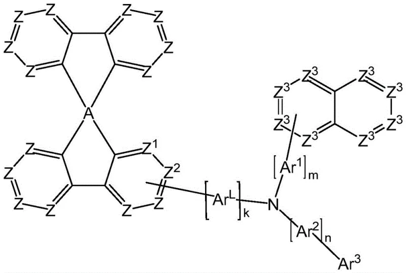
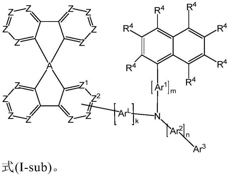
The rapid evolution of the organic electronics industry demands materials that can withstand rigorous operational stresses while maintaining peak performance metrics. Patent CN116406358A introduces a groundbreaking class of spirobifluorene amines comprising a specific aromatic or heteroaromatic ring system on the amine nitrogen atom, specifically designed to address the longevity and efficiency bottlenecks in organic electroluminescent devices. These compounds are not merely incremental improvements but represent a structural paradigm shift towards high glass transition temperature and high stability materials essential for next-generation displays. The invention targets the critical hole transporting layers and host materials within OLED stacks, where conventional materials often fail due to crystallization or thermal degradation under continuous current density. By integrating these advanced molecular architectures, manufacturers can achieve devices with drastically reduced operating voltages and significantly extended service lifetimes, meeting the stringent requirements of modern consumer electronics and lighting applications.
Historically, the reliance on standard triarylamine compounds such as simple spirobifluorene and fluorenamine has presented substantial limitations in high-performance electronic device fabrication. Conventional methods often struggle to balance the trade-off between charge carrier mobility and morphological stability, leading to premature device failure when subjected to prolonged electrical stress. The prior art materials frequently exhibit insufficient glass transition temperatures, causing unwanted crystallization within the thin film layers which disrupts the uniformity of charge transport and creates dark spots in the display panel. Furthermore, traditional synthetic routes for these legacy compounds often involve harsh conditions or generate difficult-to-remove impurities that compromise the electronic purity required for phosphorescent emitters. This technological stagnation has necessitated a search for new compounds that can act as robust hole transporting host materials without sacrificing the efficiency needed for commercial viability in competitive markets.
The novel approach detailed in the patent data overcomes these historical deficiencies by engineering a specific substitution pattern at the amine nitrogen atom of the spirobifluorene backbone. This structural modification introduces significant steric bulk and electronic tuning capabilities that prevent molecular packing and crystallization, thereby maintaining an amorphous state even at elevated operating temperatures. The new compounds are characterized by their ability to function effectively as hole transport materials and hole transport host materials, particularly for phosphorescent emitters which are sensitive to the surrounding matrix environment. By carefully selecting the aromatic or heteroaromatic ring systems attached to the core, the invention ensures high hole conductivity while simultaneously blocking electrons to confine excitons within the light-emitting layer. This dual functionality results in a device architecture that delivers high efficiency and long lifetime, solving the critical pain points of voltage rise and luminance decay observed in earlier generations of organic electronic materials.
Mechanistic Insights Into Spirobifluorene Amine Charge Transport
The exceptional performance of these materials stems from the precise manipulation of molecular orbitals through the strategic placement of substituents on the spirobifluorene core. The spiro-structure itself provides a three-dimensional rigidity that inhibits close packing of molecules, which is the primary mechanism for achieving high glass transition temperatures and thermal stability. When the amino group is bonded to specific positions on the spirobifluorene ring system, it creates a pathway for efficient hole injection from the anode while maintaining a high energy LUMO level to prevent electron leakage. The presence of specific aromatic ring systems, such as naphthyl or biphenyl groups, further delocalizes the electron density, reducing the reorganization energy during charge transfer events. This mechanistic advantage ensures that the material can sustain high current densities without undergoing electrochemical degradation, which is a common failure mode in less stable organic semiconductors used in mass production today.
Impurity control is another critical aspect of the mechanistic design, as trace contaminants can act as quenching sites that reduce luminescence efficiency. The synthetic pathways described allow for the use of highly selective palladium-catalyzed coupling reactions which minimize the formation of side products compared to older condensation methods. The resulting compounds can be purified to electronic grade standards through sublimation, a process that removes non-volatile impurities and residual catalysts that could otherwise degrade device performance over time. The structural integrity of the spirobifluorene amine ensures that even under the high electric fields present in an operating OLED, the molecule does not undergo bond cleavage or rearrangement. This chemical robustness translates directly to the macroscopic reliability of the electronic device, ensuring that the initial efficiency metrics are maintained throughout the operational lifespan of the product, which is a key requirement for automotive and premium display applications.
How To Synthesize Spirobifluorene Amines Efficiently
The synthesis of these high-value electronic chemicals relies on robust organometallic coupling strategies that are well-established in fine chemical manufacturing yet optimized here for maximum purity and yield. The process typically begins with the preparation of halogen-substituted spirobifluorene intermediates which serve as the electrophilic coupling partners in subsequent reactions. Detailed standardized synthesis steps see the guide below which outlines the specific reaction conditions and workup procedures necessary to achieve the required purity profiles. By adhering to these protocols, manufacturers can ensure batch-to-batch consistency which is vital for qualifying materials in the supply chains of major electronics corporations. The flexibility of the synthetic route allows for the introduction of various functional groups, enabling the customization of material properties to suit specific device architectures without requiring a complete redesign of the manufacturing process.
- Prepare halogen-substituted spirobifluorene or fluorenone precursors through standard halogenation or oxidation processes ensuring high purity.
- Execute Palladium-catalyzed Buchwald or Suzuki coupling reactions with specific diarylamine or boronic acid derivatives under inert atmosphere.
- Purify the crude product via recrystallization and final vacuum sublimation to achieve electronic grade purity exceeding 99.9 percent.
Commercial Advantages For Procurement And Supply Chain Teams
From a procurement perspective, the adoption of this technology offers substantial opportunities for cost optimization and supply chain resilience in the manufacturing of electronic chemicals. The synthetic routes utilize readily available starting materials and common catalysts, reducing the dependency on exotic reagents that are subject to volatile market pricing and supply disruptions. This accessibility ensures a stable supply of raw materials, allowing for consistent production scheduling and reliable delivery timelines to downstream device manufacturers. Furthermore, the high purity achievable through the described purification methods reduces the rate of device failure during quality assurance testing, effectively lowering the total cost of ownership for the end user. By minimizing waste and improving yield through optimized reaction conditions, the overall manufacturing footprint is reduced, aligning with global sustainability goals and regulatory compliance standards.
- Cost Reduction In Manufacturing: The elimination of complex multi-step purification sequences required for less stable analogues leads to significant processing cost savings. By utilizing efficient coupling reactions that proceed with high selectivity, the need for extensive chromatographic separation is minimized, which drastically reduces solvent consumption and labor hours. The ability to achieve high purity via sublimation rather than multiple recrystallization steps further streamlines the production workflow, lowering energy consumption and equipment wear. These efficiencies compound to create a more economical production model that can withstand price pressure in the competitive electronic materials market without compromising on quality standards.
- Enhanced Supply Chain Reliability: The reliance on standard organometallic chemistry means that the production process can be easily replicated across multiple manufacturing sites, mitigating the risk of single-source bottlenecks. The stability of the intermediates allows for safer storage and transportation, reducing the logistical complexities associated with hazardous or unstable chemicals. This robustness ensures that lead times remain predictable even during periods of high demand, providing procurement managers with the confidence to plan long-term inventory strategies. The scalability of the process from laboratory to industrial scale ensures that supply can be ramped up quickly to meet the needs of new product launches in the consumer electronics sector.
- Scalability And Environmental Compliance: The synthetic methods described are amenable to large-scale batch processing, facilitating the transition from pilot plant to full commercial production with minimal technical risk. The use of recoverable solvents and the reduction of heavy metal waste through efficient catalyst management align with strict environmental regulations governing chemical manufacturing. This compliance reduces the regulatory burden on the supply chain and prevents costly shutdowns due to environmental violations. Additionally, the high thermal stability of the final product reduces the need for specialized handling equipment during device fabrication, simplifying the integration of these materials into existing production lines.
Frequently Asked Questions (FAQ)
The following questions address common technical and commercial inquiries regarding the implementation of these spirobifluorene amines in electronic device manufacturing. These answers are derived directly from the technical specifications and performance data outlined in the patent documentation to ensure accuracy and relevance for industry professionals. Understanding these details is crucial for R&D teams evaluating new materials for their next-generation product roadmaps. The information provided here serves as a foundational reference for discussions regarding material qualification and process integration.
Q: What Are The Primary Advantages Of Spirobifluorene Amines In OLED Devices?
A: These compounds offer significantly improved glass transition temperatures and morphological stability compared to conventional triarylamines, resulting in extended device lifetime and reduced operating voltage in organic electroluminescent applications.
Q: How Does The Novel Substitution Pattern Affect Hole Transport Efficiency?
A: By bonding specific aromatic or heteroaromatic ring systems at the amine nitrogen atom on the spirobifluorene core, the material achieves optimized HOMO levels that facilitate superior hole injection and transport while maintaining thermal stability.
Q: Is This Technology Scalable For Industrial Production?
A: Yes, the synthesis relies on established organometallic coupling methods like Suzuki and Buchwald reactions which are well-suited for kilogram to ton-scale manufacturing with robust quality control measures.
Partnering With NINGBO INNO PHARMCHEM: Your Reliable Spirobifluorene Amines Supplier
As a leader in the fine chemical industry, NINGBO INNO PHARMCHEM possesses the technical expertise and infrastructure required to bring these complex molecular architectures from patent to production. We have extensive experience scaling diverse pathways from 100 kgs to 100 MT/annual commercial production, ensuring that your supply needs are met with precision and consistency. Our facilities are equipped with stringent purity specifications and rigorous QC labs capable of verifying the electronic grade quality required for OLED applications. We understand the critical nature of impurity profiles in electronic materials and employ advanced analytical techniques to guarantee that every batch meets the highest industry standards for performance and reliability.
We invite you to contact our technical procurement team to discuss how we can support your specific material requirements with a Customized Cost-Saving Analysis tailored to your production volume. Our experts are ready to provide specific COA data and route feasibility assessments to help you evaluate the integration of these advanced spirobifluorene amines into your supply chain. Partner with us to leverage our manufacturing capabilities and secure a reliable source of high-performance electronic chemicals that drive innovation in your display and lighting products.