Advanced Purification Technology for Semiconductor-Grade Alkylene Glycol Monoalkyl Ether Carboxylates
The semiconductor industry's relentless drive towards miniaturization has placed unprecedented demands on the purity of process chemicals, particularly solvents used in photolithography. Patent CN115872868A introduces a groundbreaking purification methodology for Alkylene Glycol Monoalkyl Ether Carboxylates (AGAECE), specifically targeting the rigorous standards required for EUV and ArF light source applications. As feature sizes shrink, the tolerance for impurities such as residual acids and moisture diminishes drastically, necessitating a shift from conventional recycling methods to advanced chemical purification. This patent details a sophisticated multi-stage process combining alkaline adsorption, vacuum distillation, and ion exchange to transform industrial-grade feedstock into semiconductor-grade solvents. By addressing the critical pain points of acid value control and impurity removal, this technology offers a viable pathway for reliable semiconductor solvent supplier networks to meet the escalating quality benchmarks of modern integrated circuit manufacturing.
The Limitations of Conventional Methods vs. The Novel Approach
The Limitations of Conventional Methods
Traditional approaches to obtaining high-purity solvents often rely on the recycling and purification of waste streams generated during LCD panel manufacturing. However, these legacy methods face significant hurdles when applied to the more sensitive semiconductor fabrication environment. Waste solvents recovered from LCD processes inherently contain a complex matrix of contaminants that are difficult to separate completely, often resulting in products that fail to meet the stringent < 20ppm acid value requirement for advanced lithography. Furthermore, simple distillation of these recycled streams can sometimes exacerbate impurity profiles due to thermal degradation or incomplete separation of azeotropic mixtures. The reliance on variable quality waste feedstock introduces supply chain volatility and inconsistency, making it challenging for procurement teams to guarantee the batch-to-batch reproducibility essential for high-yield wafer production. Consequently, the industry requires a more robust synthesis and purification strategy that starts with defined industrial raw materials rather than unpredictable waste streams.
The Novel Approach
The innovation disclosed in CN115872868A circumvents these limitations by utilizing a targeted chemical treatment of industrial-grade AGAECE rather than relying solely on physical separation of waste. The core of this novel approach lies in the use of a porous adsorbent impregnated with specific alkaline substances, such as sodium hydroxide or potassium hydroxide. This engineered adsorbent acts as a selective scavenger, effectively neutralizing residual carboxylic acids and absorbing moisture without inducing hydrolysis of the valuable ester solvent. Following this adsorption step, the process incorporates a vacuum distillation stage enhanced with antioxidants to prevent thermal oxidation, and finally, a polishing step using basic ion exchange resins. This comprehensive strategy ensures that the final product maintains a purity level exceeding 99.99% while suppressing acid values to single-digit ppm levels, thereby establishing a new benchmark for cost reduction in electronic chemical manufacturing.
Mechanistic Insights into Alkaline Adsorption and Ester Stability
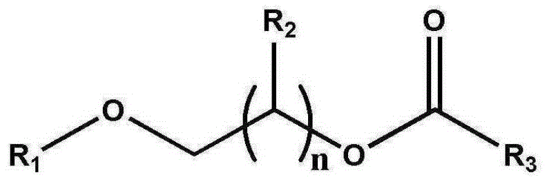
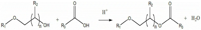
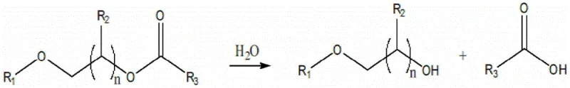
The chemical stability of AGAECE compounds, such as Propylene Glycol Methyl Ether Acetate (PGMEA), is paramount during purification. These molecules possess an ester linkage that is susceptible to hydrolysis in the presence of water and acid or base catalysts. The patent elucidates the delicate balance required to remove acidic impurities without triggering the decomposition of the solvent itself. As illustrated in the general synthesis and degradation pathways, AGAECE is typically formed via the esterification of an alkylene glycol monoalkyl ether with a carboxylic acid. However, the reverse reaction, hydrolysis, can regenerate the parent alcohol and acid, introducing the very impurities the process aims to eliminate. The novelty of the described method is the immobilization of the base on a porous support. By fixing the alkaline species (e.g., OH-) onto a solid matrix like activated carbon or zeolite, the system creates a heterogeneous environment where acid neutralization occurs at the surface interface. This minimizes the exposure of the bulk liquid solvent to free strong bases that would otherwise catalyze rapid ester hydrolysis, thus preserving the integrity of the high-purity photoresist solvent.
Furthermore, the mechanism addresses the generation of impurities during the thermal stress of distillation. Even trace amounts of moisture remaining after adsorption can lead to hydrolysis at elevated temperatures, generating propylene glycol methyl ether (PM) as a byproduct. To counteract this, the process mandates the addition of antioxidants during the distillation phase. Phenolic antioxidants like BHT or TBC act as radical scavengers, interrupting the chain reactions that lead to oxidative degradation and coloration of the solvent. This dual-protection strategy—chemical neutralization of acids followed by radical inhibition during thermal separation—ensures that the impurity profile remains tightly controlled. The subsequent passage through a strong basic ion exchange resin serves as a final polishing mechanism, capturing any trace acidic species that may have formed or survived the earlier steps, guaranteeing the ultra-low acidity required for preventing corrosion in semiconductor processing equipment.
How to Synthesize High-Purity PGMEA Efficiently
The synthesis and purification protocol outlined in the patent provides a scalable route for producing semiconductor-grade solvents suitable for critical lithography steps. The process begins with the preparation of the functionalized adsorbent, where a porous carrier is impregnated with an alkaline solution and calcined to ensure stable binding. Industrial grade feedstock is then passed through this column at a optimized space velocity to maximize acid removal while maintaining throughput. The effluent is subsequently subjected to vacuum distillation under an inert atmosphere with antioxidant protection to separate volatile impurities and residual moisture. Finally, the distilled solvent is polished through an ion exchange column to achieve the target specifications. For detailed operational parameters and specific equipment configurations, the standardized synthesis steps are provided below.
- Impregnate a porous adsorbent (such as activated carbon or zeolite) with an alkaline substance like NaOH or KOH and calcine it.
- Pass industrial-grade AGAECE through the alkaline porous adsorbent at a controlled space velocity (SV=1 to 8) to reduce acid value.
- Perform vacuum distillation on the treated AGAECE with added antioxidants, followed by passing through a basic ion exchange resin.
Commercial Advantages for Procurement and Supply Chain Teams
For procurement managers and supply chain directors, the adoption of this purification technology translates into tangible strategic benefits beyond mere technical specifications. By shifting the raw material basis from unpredictable waste streams to consistent industrial-grade feedstock, manufacturers can significantly stabilize their supply chains and reduce the risk of production stoppages due to off-spec materials. The ability to consistently produce solvents with acid values below 20ppm directly correlates to higher yields in wafer fabrication, as it minimizes the risk of pattern defects and equipment corrosion. This reliability allows for longer maintenance intervals on expensive lithography tools and reduces the total cost of ownership for semiconductor fabs. Moreover, the process eliminates the need for complex and costly post-treatment steps often associated with recycled solvents, streamlining the manufacturing workflow and enhancing overall operational efficiency.
- Cost Reduction in Manufacturing: The implementation of this alkaline adsorption and distillation hybrid process offers substantial cost savings by optimizing raw material utilization. Unlike traditional recycling which suffers from yield losses due to the rejection of heavily contaminated batches, this method tolerates a wider range of initial feedstock quality while still achieving semiconductor-grade output. The use of regenerable or cost-effective adsorbents like activated carbon further drives down variable costs. Additionally, by preventing the formation of hydrolysis byproducts through controlled conditions, the process maximizes the recovery of the valuable ester solvent, ensuring that less material is wasted as off-spec byproduct. This efficiency gain contributes to a more competitive pricing structure for high-purity electronic chemicals without compromising on quality standards.
- Enhanced Supply Chain Reliability: Dependence on waste solvent streams from the LCD industry creates a vulnerable supply chain subject to the fluctuations of a different market sector. By utilizing industrial-grade AGAECE as the primary feedstock, suppliers can decouple their production capacity from the volatility of the display panel market. This independence ensures a more predictable and continuous supply of critical lithography solvents, which is essential for maintaining the just-in-time delivery schedules demanded by major semiconductor foundries. The robustness of the purification process also means that inventory holding times can be managed more effectively, as the product stability is enhanced by the rigorous removal of destabilizing acidic impurities, reducing the risk of shelf-life degradation during storage and transit.
- Scalability and Environmental Compliance: The described purification method is inherently scalable, utilizing unit operations such as fixed-bed adsorption and fractional distillation that are well-understood and easily expanded from pilot to commercial scale. This facilitates the commercial scale-up of complex fine chemicals required for the growing demand in advanced node manufacturing. From an environmental perspective, the process minimizes the generation of hazardous waste compared to aggressive chemical washing methods. The use of solid adsorbents reduces the volume of aqueous waste streams, and the efficient recovery of solvents aligns with green chemistry principles. This compliance with increasingly stringent environmental regulations enhances the corporate sustainability profile of manufacturers, making them more attractive partners for eco-conscious global technology corporations.
Frequently Asked Questions (FAQ)
The following questions address common technical and commercial inquiries regarding the implementation and benefits of this advanced purification technology. These insights are derived directly from the experimental data and process descriptions within the patent documentation, providing clarity on how this method outperforms conventional techniques. Understanding these nuances is critical for technical teams evaluating new solvent sources for their fabrication lines. The answers highlight the specific mechanisms by which acid values are controlled and purity is maintained, offering confidence in the reproducibility of the results.
Q: Why is low acid value critical for EUV/ArF photoresist solvents?
A: High acid content in solvents like PGMEA can corrode semiconductor equipment and react with alkaline developers (e.g., TMAH), leading to chip defects and inconsistent pattern formation in fine-line lithography.
Q: How does the alkaline adsorbent method differ from traditional recycling?
A: Unlike traditional recycling of waste solvents which often retain LCD-grade impurities, this method uses fresh industrial feedstock treated with specific alkaline adsorbents to selectively neutralize acids without degrading the ester structure.
Q: What purity levels are achievable with this purification technology?
A: The process achieves semiconductor-grade purity exceeding 99.99% with acid values reduced to below 20ppm, and potentially below 10ppm after ion exchange, meeting strict EUV process requirements.
Partnering with NINGBO INNO PHARMCHEM: Your Reliable PGMEA Supplier
As the demand for ultra-high purity solvents continues to surge with the adoption of EUV lithography, partnering with a manufacturer that possesses deep technical expertise in purification is essential. NINGBO INNO PHARMCHEM stands at the forefront of this sector, leveraging advanced process technologies similar to those described in CN115872868A to deliver solvents that meet the most rigorous semiconductor specifications. Our facilities are equipped with state-of-the-art distillation and filtration systems, allowing us to ensure stringent purity specifications and rigorous QC labs testing for every batch. We possess extensive experience scaling diverse pathways from 100 kgs to 100 MT/annual commercial production, ensuring that we can meet your volume requirements without sacrificing the quality critical for your yield.
We invite you to collaborate with our technical team to explore how our purified AGAECE solutions can optimize your photoresist processes. By engaging with us, you gain access to a Customized Cost-Saving Analysis tailored to your specific consumption patterns and purity requirements. We encourage you to contact our technical procurement team to request specific COA data and route feasibility assessments, ensuring that your supply chain is built on a foundation of quality, reliability, and scientific excellence.