Advanced Cross-Linkable Hole Transport Materials for Next-Generation OLED and QLED Displays
The rapid evolution of the display industry towards high-resolution, flexible, and large-area screens has necessitated a paradigm shift in the manufacturing of organic light-emitting diodes (OLEDs) and quantum dot light-emitting diodes (QLEDs). Patent CN108794380B introduces a groundbreaking class of hole transport materials (HTMs) designed specifically to overcome the limitations of traditional vacuum evaporation processes by enabling robust solution processing techniques. This innovation centers on novel compounds featuring a bis-spirofluorene core functionalized with cross-linkable groups, which allow for the creation of solvent-resistant thin films essential for multilayer device architectures. As a reliable OLED material supplier, understanding the nuances of this technology is critical for stakeholders aiming to reduce production costs while enhancing device performance through advanced chemical engineering.
The transition from vacuum evaporation to solution processing represents a significant technological leap, yet it has historically been plagued by the issue of interlayer mixing. In conventional solution-processed OLEDs, the deposition of an upper organic layer often involves solvents that can dissolve or damage the underlying functional layers, leading to increased surface roughness and device failure. The materials disclosed in this patent address this fundamental challenge by incorporating polymerizable vinyl groups that, upon thermal treatment, form a tightly cross-linked network. This network exhibits exceptional resistance to common organic solvents such as toluene and chlorobenzene, thereby preserving the integrity of the hole transport layer during the subsequent deposition of emission and electron transport layers. This capability is pivotal for the commercial viability of inkjet printing and spin-coating technologies in mass production environments.
The Limitations of Conventional Methods vs. The Novel Approach
The Limitations of Conventional Methods
Traditional manufacturing of OLED displays predominantly relies on vacuum thermal evaporation (VTE), a process that, while mature, suffers from severe economic and material efficiency drawbacks. The VTE technique typically utilizes single-point evaporation sources which result in a material utilization rate of merely 5%, meaning 95% of the expensive organic semiconductor material is wasted during deposition. Furthermore, the equipment investment and maintenance costs for vacuum systems are prohibitively high, creating a significant barrier to entry for large-area display manufacturing. Although line-type evaporation sources have marginally improved utilization, they still cannot compete with the theoretical efficiency of solution-based methods. Additionally, small molecule materials processed via solution methods without cross-linking capabilities lack the mechanical and chemical stability required for multilayer stacking, limiting their application to single-layer or simplified device structures that fail to meet the performance standards of modern high-end displays.
The Novel Approach
The novel approach presented in the patent leverages a unique molecular architecture that combines the ease of small molecule synthesis with the durability of cross-linked polymers. By synthesizing compounds based on a double-spirofluorene core and attaching specific cross-linking groups (such as vinylphenyl moieties), the material remains soluble in organic solvents prior to curing, allowing for uniform film formation via spin-coating or inkjet printing. Once the film is formed, a thermal curing step triggers the polymerization of the vinyl groups, locking the molecules into a rigid, insoluble network. This transformation effectively 'freezes' the hole transport layer, rendering it impervious to the solvents used in subsequent processing steps. Consequently, this enables the fabrication of complex, multilayer OLED and QLED structures entirely through solution methods, drastically reducing material waste to less than 10% and eliminating the need for expensive vacuum infrastructure, thus offering a clear pathway for cost reduction in electronic chemical manufacturing.
Mechanistic Insights into Suzuki-Miyaura Coupling and Thermal Cross-Linking
The synthesis of these advanced hole transport materials relies heavily on palladium-catalyzed cross-coupling reactions, specifically the Suzuki-Miyaura coupling, to construct the complex aromatic framework. The core bis-spirofluorene structure is functionalized with boronic acid groups, which then react with brominated aryl amine derivatives in the presence of a palladium catalyst such as tetrakis(triphenylphosphine)palladium. This reaction proceeds under mild conditions, typically in a mixture of toluene and ethanol with an aqueous base like potassium carbonate, facilitating the formation of robust carbon-carbon bonds between the electron-rich amine units and the spirofluorene core. The precision of this coupling is essential for maintaining the high purity required for electronic applications, as trace metal impurities or structural defects can act as quenching sites that degrade device efficiency. Following the construction of the core scaffold, further functionalization introduces the cross-linkable vinyl groups, completing the molecular design.
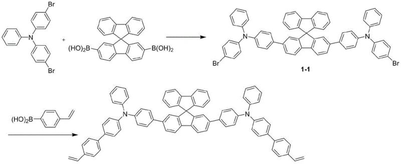
Upon thermal activation, typically at temperatures around 230°C, the pendant vinyl groups undergo a free-radical polymerization or addition reaction. This process creates covalent bonds between adjacent molecules, transforming the discrete small molecules into a continuous macromolecular network. This cross-linking mechanism is crucial not only for solvent resistance but also for enhancing charge carrier mobility. The rigidification of the molecular structure reduces conformational disorder and facilitates more efficient pi-orbital overlap between adjacent units, thereby improving the hopping rate of holes through the transport layer. The resulting material exhibits the best of both worlds: the definable structure and high purity of a small molecule prior to curing, and the mechanical stability and solvent resistance of a polymer post-curing, making it an ideal candidate for high-performance electroluminescent devices.
How to Synthesize Cross-Linkable Spirofluorene Derivatives Efficiently
The synthesis protocol outlined in the patent provides a reproducible method for generating these high-value intermediates and final products. The process begins with the preparation of key intermediates via Suzuki coupling, followed by purification steps to ensure electronic-grade quality. The final functionalization step introduces the reactive vinyl groups necessary for the cross-linking property. Detailed operational parameters, including stoichiometry, temperature profiles, and purification techniques, are critical for achieving the high yields and purity levels reported in the examples. For a comprehensive guide on executing this synthesis in a GMP-compliant environment, please refer to the standardized procedure below.
- Perform a palladium-catalyzed Suzuki coupling reaction between a bis-spirofluorene diboronic acid derivative and brominated aryl amine precursors to form the core intermediate structure.
- Execute a second coupling reaction or functionalization step to introduce vinyl-containing groups onto the periphery of the molecule, enabling subsequent thermal cross-linking.
- Purify the final small molecule product via silica gel column chromatography to ensure high purity suitable for solution processing and device fabrication.
Commercial Advantages for Procurement and Supply Chain Teams
For procurement managers and supply chain directors, the adoption of these cross-linkable hole transport materials offers transformative economic benefits that extend beyond simple material costs. The shift from vacuum evaporation to solution processing fundamentally alters the capital expenditure (CAPEX) and operational expenditure (OPEX) models of display manufacturing. By enabling the use of inkjet printing and roll-to-roll coating technologies, manufacturers can significantly reduce the reliance on high-vacuum chambers and complex masking equipment. This transition not only lowers the initial investment in production lines but also simplifies the maintenance requirements, leading to higher uptime and overall equipment effectiveness (OEE). Furthermore, the dramatic improvement in material utilization rates—from single digits in evaporation to over 90% in printing—directly translates to substantial cost savings in raw material consumption, which is particularly impactful given the high price of specialized organic semiconductors.
- Cost Reduction in Manufacturing: The elimination of vacuum evaporation steps removes the need for expensive high-vacuum pumps and shielding materials, which are significant cost drivers in traditional OLED production. Additionally, the high material utilization rate of solution processing means that less raw material is required to produce the same number of display panels. This efficiency gain allows for a drastic reduction in the cost per unit area of the active layers, making large-area displays like OLED TVs more economically viable. The ability to cure the material thermally also simplifies the process flow, reducing energy consumption associated with maintaining high vacuum conditions over long periods.
- Enhanced Supply Chain Reliability: Solution-processable materials are generally easier to handle and store compared to some sensitive vacuum-deposition materials, simplifying logistics and inventory management. The robust nature of the cross-linked films ensures higher yield rates in downstream device assembly, reducing the variability in supply caused by manufacturing defects. Moreover, the scalability of solution processing techniques aligns well with existing supply chain infrastructures for liquid chemicals, allowing for smoother integration and reduced lead times for high-purity electronic chemicals. This reliability is crucial for meeting the demanding production schedules of consumer electronics giants.
- Scalability and Environmental Compliance: The solution-based manufacturing process generates significantly less solid waste compared to vacuum evaporation, where unused material coats the chamber walls and must be disposed of as hazardous waste. The higher efficiency of material usage inherently reduces the environmental footprint of the manufacturing process. Furthermore, the ability to scale up solution coating processes, such as slot-die coating or inkjet printing, is well-established in other industries, facilitating a smoother transition to gigafactory-scale production. This scalability ensures that supply can meet the surging global demand for next-generation displays without the bottlenecks associated with vacuum chamber throughput.
Frequently Asked Questions (FAQ)
The following questions address common technical and commercial inquiries regarding the implementation of these novel hole transport materials. The answers are derived directly from the experimental data and structural analysis provided in the patent documentation, ensuring accuracy and relevance for technical decision-makers. Understanding these aspects is vital for evaluating the feasibility of integrating this technology into existing or new production lines.
Q: What is the primary advantage of using cross-linkable hole transport materials in OLED manufacturing?
A: The primary advantage is the ability to fabricate multilayer devices using solution processing methods like inkjet printing. Once cross-linked, the material becomes insoluble, preventing the solvent from upper layers from eroding the underlying hole transport layer, which is a critical failure mode in traditional solution-processed OLEDs.
Q: Can these spirofluorene-based materials be utilized in Quantum Dot LED (QLED) devices?
A: Yes, the patent data explicitly demonstrates the successful application of these materials in QLED devices. They exhibit excellent hole injection and transport properties while effectively confining excitons within the quantum dot emission layer, leading to high efficiency and stable electroluminescence spectra.
Q: How does the molecular design contribute to improved charge mobility?
A: The molecular design incorporates a rigid bis-spirofluorene core which promotes tight molecular stacking. Upon thermal cross-linking, this forms a robust network polymer structure that significantly enhances hole mobility compared to non-cross-linked small molecules, while maintaining the ease of purification associated with small molecule synthesis.
Partnering with NINGBO INNO PHARMCHEM: Your Reliable Cross-Linkable HTM Supplier
At NINGBO INNO PHARMCHEM, we recognize the critical role that advanced materials play in the evolution of the display industry. Our team possesses extensive experience scaling diverse pathways from 100 kgs to 100 MT/annual commercial production, ensuring that the transition from laboratory synthesis to industrial manufacturing is seamless and efficient. We are committed to delivering high-purity spirofluorene derivatives and related electronic chemicals that meet stringent purity specifications, supported by our rigorous QC labs equipped with state-of-the-art analytical instrumentation. Our expertise in palladium-catalyzed couplings and functional group transformations allows us to optimize these complex synthetic routes for maximum yield and minimal environmental impact.
We invite you to collaborate with us to explore how these innovative hole transport materials can enhance your product portfolio and reduce your manufacturing costs. Our technical procurement team is ready to provide a Customized Cost-Saving Analysis tailored to your specific production needs. Please contact us to request specific COA data and route feasibility assessments, and let us help you engineer the next generation of high-performance OLED and QLED displays.
Engineering Bottleneck?
Can't scale up this synthesis? Upload your target structure or CAS, and our CDMO team will evaluate the industrial feasibility within 24 hours. Request Evaluation →