
Custom Manufacturing, Project Outsourcing, your Trusted Partner from China
Gallium Selenide, known chemically as Ga2Se3 and identified by CAS number 12024-24-7, is a material of considerable importance in the field of infrared optics. This dark red, brittle solid, with a molecular weight of 376.33, possesses a unique transparency in the infrared spectrum, making it an ideal material for a range of specialized optical applications.
The primary utility of Gallium Selenide in infrared optics stems from its ability to transmit infrared radiation effectively. This characteristic allows for the fabrication of high-quality optical components such as lenses, windows, and prisms that are critical for technologies operating within the infrared range. These components are fundamental to the functioning of thermal imaging cameras, infrared sensors, and various spectroscopic instruments used in scientific research, industrial inspection, and security applications.
The demand for precise optical elements that can operate reliably in the infrared spectrum is high across numerous industries. Gallium Selenide meets this demand by providing a material with excellent optical clarity and durability in the IR wavelengths. The study of Gallium Selenide infrared optics enables the development of more sophisticated and accurate imaging and sensing systems.
In addition to its optical applications, Gallium Selenide also functions as a semiconductor, finding use in photodetectors and photovoltaic cells. This dual functionality further enhances its value in integrated systems where optical detection and electronic processing are closely linked.
For professionals in optics and related fields, understanding the properties and applications of Gallium Selenide is essential. Accessing reliable information and sourcing from reputable high purity Gallium Selenide suppliers ensures the quality and performance necessary for advanced optical designs.
In conclusion, Gallium Selenide (Ga2Se3) is an indispensable material in infrared optics, enabling the creation of critical components that drive innovation in thermal imaging, sensing, and scientific instrumentation. Its unique optical and semiconductor properties solidify its importance in modern technological advancements.
Manufacturing Facilities
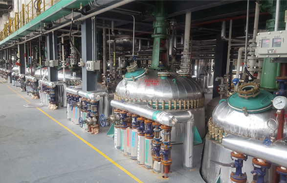
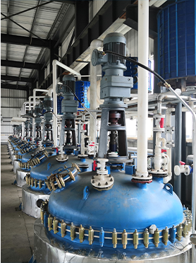
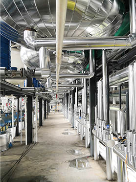
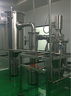
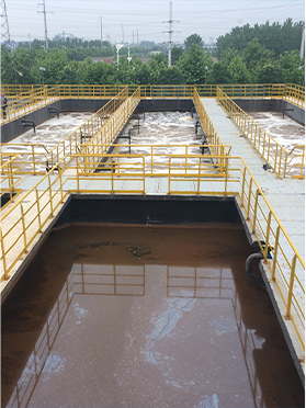
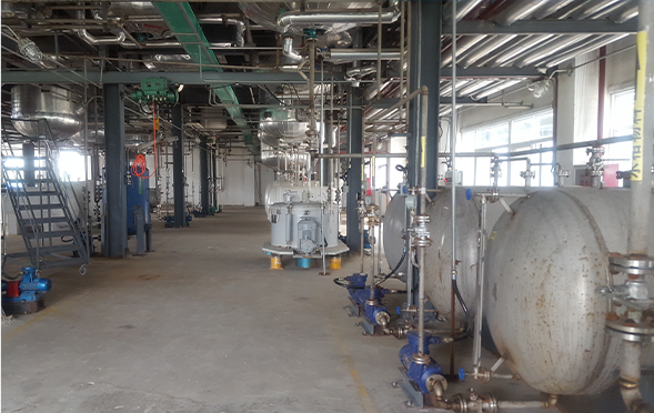
Professional Export Experience
to Global Customers
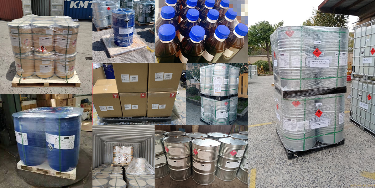
1. 20 years of R&D, manufacturing and sales experience, serving customers in 60 countries and regions around the world;
2. Own R&D laboratory, pilot platform and large-scale production workshop, which can meet the audit requirements of global customers;
3. We can satisfy customers' perfect transition from small scale lab requirements (gram level) to commercialization requirements (hundred tons level).
A: We don't have Minimum Order Quantity, exact quantity should be provided before quotation for us to calculate the exact cost.
A: We don't provide free samples due to lots of request and expensive international courier's cost, we can deduct the sample charge after commercial order placed.
A: Our payment terms: Small or sample order: T/T IN ADVANCE. Commercial order: First order should be by T/T IN ADVANCE or L/C at sight, and following orders T/T 30~90days is acceptable subject to approval of credit application.