
Custom Manufacturing, Project Outsourcing, your Trusted Partner from China
The electronics industry is constantly seeking materials that offer superior electrical conductivity, faster performance, and greater flexibility. Multi-Walled Carbon Nanotubes (MWCNTs) are at the forefront of this revolution, providing a unique combination of properties that are transforming electronic device design and functionality.
At the heart of MWCNTs' utility in electronics lies their exceptional electrical conductivity. Derived from their unique structure—a rolled-up sheet of graphene with multiple concentric layers—MWCNTs possess a delocalized electron system that facilitates efficient charge transport. This makes them highly effective in applications where electrical pathways are critical, such as in conductive inks, transistors, and transparent conductive films.
In the realm of flexible electronics and touchscreens, MWCNTs are proving to be a viable alternative to traditional materials like Indium Tin Oxide (ITO). Unlike brittle ITO, MWCNTs can be processed from solutions and deposited as flexible films, offering greater durability and adaptability for curved or foldable displays. Their ability to form a conductive network, even at low concentrations, means they can achieve high conductivity with minimal material, which is crucial for miniaturization and efficiency.
Furthermore, the semiconducting properties of some MWCNTs, coupled with their nanoscale dimensions, make them ideal candidates for advanced transistors and sensors. Researchers are actively developing MWCNT-based field-effect transistors (CNTFETs) that promise faster switching speeds and lower power consumption compared to silicon-based counterparts. The potential for precise control over these properties through synthesis and functionalization opens up avenues for creating highly sensitive sensors and novel electronic components.
As the demand for more advanced and integrated electronic systems grows, the role of MWCNTs will only become more pronounced. Their inherent conductivity, combined with ongoing research into improving their synthesis and processing, positions them as a key material for the future of electronics, driving innovation from consumer devices to specialized industrial applications.
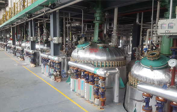
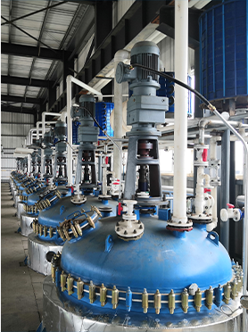
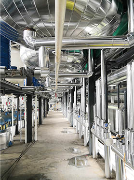
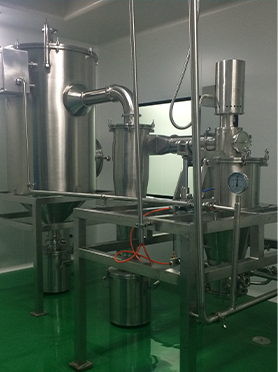
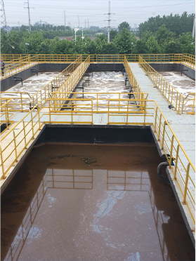
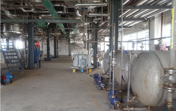
Manufacturing Facilities
Professional Export Experience
to Global Customers
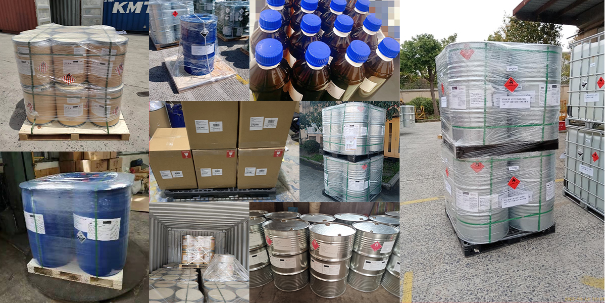
1. 20 years of R&D, manufacturing and sales experience, serving customers in 60 countries and regions around the world;
2. Own R&D laboratory, pilot platform and large-scale production workshop, which can meet the audit requirements of global customers;
3. We can satisfy customers' perfect transition from small scale lab requirements (gram level) to commercialization requirements (hundred tons level).
A: We don't have Minimum Order Quantity, exact quantity should be provided before quotation for us to calculate the exact cost.
A: We don't provide free samples due to lots of request and expensive international courier's cost, we can deduct the sample charge after commercial order placed.
A: Our payment terms: Small or sample order: T/T IN ADVANCE. Commercial order: First order should be by T/T IN ADVANCE or L/C at sight, and following orders T/T 30~90days is acceptable subject to approval of credit application.