Advanced Fluorene-Anthracene Copolymers for High Efficiency Organic Electronics Manufacturing
Advanced Fluorene-Anthracene Copolymers for High Efficiency Organic Electronics Manufacturing
Introduction to Patent CN102453228A Technology
The technological landscape of organic electronics is undergoing a significant transformation with the introduction of advanced copolymer architectures described in patent CN102453228A. This intellectual property discloses a novel organic semiconductor material containing fluorene, anthracene, and benzodithiophene units, specifically engineered to overcome the efficiency bottlenecks of previous generation materials. By integrating these distinct conjugated systems into a single polymer backbone, the invention achieves a synergistic effect that enhances carrier mobility, broadens the light absorption range, and improves overall sunlight utilization rates. This breakthrough is particularly critical for the development of next-generation organic solar cells and optoelectronic devices where performance and cost-efficiency are paramount. The structural versatility of the material allows for precise tuning of electronic properties through variable alkyl side chains, offering a robust platform for high-performance electronic applications that demand both stability and high quantum yield.
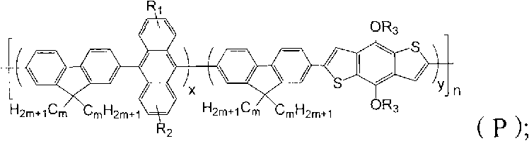
The strategic combination of these three specific units addresses the fundamental limitations of single-component organic semiconductors. Fluorene provides structural rigidity and chemical stability, while anthracene contributes superior hole transport characteristics and film-forming properties. The inclusion of benzodithiophene units introduces a strong electron-donating effect and symmetry that effectively regulates the band gap of the semiconductor. This regulation pushes the energy absorption edge towards the infrared and near-infrared regions, ensuring that a wider spectrum of solar radiation is captured and converted into electrical energy. For R&D directors and technical procurement managers, this material represents a viable pathway to achieving power conversion efficiencies that rival inorganic counterparts while retaining the inherent benefits of organic processing, such as flexibility and lightweight design.
The Limitations of Conventional Methods vs. The Novel Approach
The Limitations of Conventional Methods
Historically, high-efficiency solar cells have relied heavily on inorganic semiconductor materials, with silicon wafers dominating the market despite significant drawbacks in their production lifecycle. The manufacturing process for silicon-based cells is notoriously complex, energy-intensive, and generates substantial environmental pollution, which has severely suppressed the development of their cost-effective commercial applications on a global scale. While organic semiconductor materials emerged as an attractive alternative due to their lower preparation costs and environmental stability, early iterations suffered from relatively low carrier mobility and narrow spectral response ranges. These limitations meant that the spectral response of the devices did not match the solar radiation spectrum effectively, leaving the red light district of high photon flux largely unused and resulting in low electrode collection efficiency for current carriers. Consequently, the efficiency of conversion for organic solar cells remained much lower than that of inorganic cells, restricting their practical deployment in high-performance energy harvesting applications.
The Novel Approach
The novel approach presented in this patent overcomes these barriers by strategically combining the planar rigidity of fluorene with the excellent stability and film-forming properties of anthracene and benzodithiophene. This ternary copolymer system leverages the strong electron-donating effect of the benzodithiophene unit and the high hole mobility of anthracene to create a material with superior charge transport characteristics. The resulting polymer exhibits a lower energy gap and wider absorption bandwidth, significantly improving the photoelectric conversion efficiency while maintaining the inherent advantages of solution-processable organic materials. By modifying the benzodithiophene unit with alkyl chains, the inventors have also improved the solubility and processing characteristics of the polymer, enabling the realization of large-area manufacturing on flexible substrates. This holistic design ensures that the material is not only theoretically efficient but also practically viable for industrial-scale production of cheap and attractive solar cell modules.
Mechanistic Insights into Suzuki-Catalyzed Polymerization
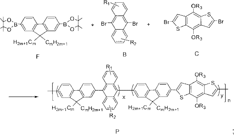
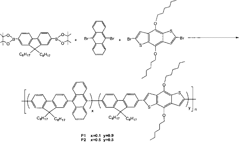
The synthesis of this advanced organic semiconductor relies heavily on the Suzuki-Miyaura cross-coupling reaction, a palladium-catalyzed process that links the boronated fluorene derivative with brominated anthracene and benzodithiophene monomers. This mechanism ensures the formation of a well-defined conjugated backbone with precise control over the molecular weight and polydispersity, which are critical factors for consistent device performance across different batches. The reaction conditions, typically involving a palladium catalyst like Pd(PPh3)4 and a base such as Na2CO3 in a toluene solvent system, facilitate the efficient coupling of the monomeric units under anhydrous and oxygen-free environments. Maintaining these strict conditions is essential to prevent catalyst deactivation and ensure high yield, as the presence of oxygen or moisture can lead to side reactions that compromise the integrity of the conjugated system and reduce the overall carrier mobility of the final polymer.
Impurity control is meticulously managed through a multi-step purification protocol that includes precipitation in methanol, chromatography column separation, and extensive Soxhlet extraction. These steps are essential for removing residual palladium catalysts and unreacted monomers that could act as charge traps within the semiconductor layer, thereby degrading device efficiency. The rigorous purification ensures that the final polymer meets stringent purity specifications required for high-performance organic field-effect transistors and solar cells. For technical teams, understanding this purification workflow is crucial, as the removal of metal residues is directly correlated with the longevity and stability of the electronic device. The patent details specific solvent systems and extraction times that optimize the monodispersity of the polymer molecular weight, ensuring uniform film formation and consistent electronic properties throughout the active layer of the device.
How to Synthesize Fluorene-Anthracene Copolymers Efficiently
The synthesis pathway outlined in the patent provides a clear roadmap for producing these high-value materials with high yield and operational controllability. The process begins with the preparation of key intermediates, such as 2,7-dibromo-9,9-dialkylfluorene, which are then converted into reactive boronate esters suitable for polymerization. The detailed standardized synthesis steps see the guide below, which outlines the precise molar ratios, temperature controls, and reaction times necessary to achieve the target molecular weights. Adhering to these parameters is critical for reproducing the high carrier mobility and wide light absorption properties described in the technical data. This section serves as a foundational reference for process engineers looking to adapt this laboratory-scale method for commercial production environments.
- Prepare 2,7-dibromo-9,9-dialkylfluorene and convert to bis-boronate ester using n-BuLi and pinacol boronic ester under anhydrous conditions.
- Mix the fluorene bis-boronate with 9,10-dibromoanthracene and dibromo-benzodithiophene derivatives in a specific molar ratio.
- Perform Suzuki polymerization using a palladium catalyst and base in toluene at 70-100°C, followed by purification via precipitation and Soxhlet extraction.
Commercial Advantages for Procurement and Supply Chain Teams
The transition to this specific copolymer architecture offers substantial economic benefits by simplifying the manufacturing workflow and utilizing readily available chemical feedstocks. The elimination of complex vacuum deposition steps required for inorganic semiconductors allows for solution-based processing techniques like spin coating or inkjet printing, which drastically reduces capital expenditure and operational costs associated with device fabrication. Furthermore, the high yield and operational controllability of the Suzuki coupling reaction ensure a consistent supply of high-quality material, mitigating the risks of production bottlenecks that often plague specialty chemical supply chains. For procurement managers, this translates into a more predictable cost structure and a reliable source of high-performance materials that can be sourced without dependency on rare earth minerals or geopolitically constrained resources.
- Cost Reduction in Manufacturing: The synthetic route avoids the use of expensive transition metal catalysts in the final product through effective purification, eliminating the need for costly heavy metal removal steps often required in pharmaceutical-grade intermediates. By utilizing standard organic solvents and common reagents like n-Butyl Lithium and pinacol boronic esters, the process minimizes raw material expenses while maintaining high reaction efficiency. This streamlined approach translates into significant cost savings for large-scale production, making high-performance organic electronics more accessible for mass-market applications without compromising on material quality. The ability to tune the band gap through simple monomer ratio adjustments further allows for cost optimization without the need for complex new synthetic routes.
- Enhanced Supply Chain Reliability: The starting materials, including dibromoanthracene and benzodithiophene derivatives, are commercially accessible and do not rely on rare or geopolitically constrained resources. This abundance ensures a stable supply chain capable of meeting fluctuating market demands without the volatility associated with scarce mineral extraction. Additionally, the robustness of the polymerization process allows for flexible manufacturing schedules, enabling suppliers to respond quickly to urgent procurement requests and maintain continuous production lines even during periods of high market volatility. The chemical stability of the final polymer also ensures long shelf-life, reducing waste and inventory management costs for downstream manufacturers.
- Scalability and Environmental Compliance: The solution-processable nature of the material facilitates easy scale-up from laboratory grams to industrial tons using standard chemical reactor infrastructure. The process generates manageable waste streams that can be treated using conventional methods, aligning with increasingly strict environmental regulations regarding industrial chemical discharge. This scalability ensures that the material can support the growing demand for organic photovoltaics and flexible displays while adhering to global sustainability standards. The ability to produce these materials with a lower carbon footprint compared to silicon-based alternatives provides a future-proof solution for eco-conscious manufacturing partners seeking to reduce their overall environmental impact.
Frequently Asked Questions (FAQ)
The following questions and answers are derived directly from the technical specifications and beneficial effects detailed in the patent documentation. They address common concerns regarding material performance, synthesis feasibility, and application potential. Understanding these technical nuances is essential for stakeholders evaluating the integration of this material into their existing product lines or research pipelines. The answers reflect the objective capabilities of the technology as demonstrated in the provided examples and comparative data.
Q: How does the anthracene unit improve carrier mobility in this material?
A: The anthracene unit provides excellent planarity and conjugation degree within the polymer backbone, which significantly enhances hole mobility and charge transport characteristics compared to traditional fluorene-only polymers.
Q: What modifications improve the solubility of the benzodithiophene unit?
A: Introducing alkyl chains, such as hexyloxy or octyloxy groups, onto the benzodithiophene unit improves the solubility and processibility of the conjugated polymer, facilitating solution-based fabrication methods.
Q: What are the primary applications for this organic semiconductor material?
A: This material is designed for use in organic solar cells, organic electroluminescent devices (OLEDs), organic field-effect transistors (OFETs), and organic laser apparatus due to its wide light absorption and high carrier mobility.
Partnering with NINGBO INNO PHARMCHEM: Your Reliable Organic Semiconductor Material Supplier
As a leader in the fine chemical industry, NINGBO INNO PHARMCHEM possesses the technical expertise and infrastructure to support the commercialization of advanced materials like the fluorene-anthracene copolymers described in CN102453228A. Our team has extensive experience scaling diverse pathways from 100 kgs to 100 MT/annual commercial production, ensuring that laboratory innovations can be seamlessly transitioned into industrial reality. We maintain stringent purity specifications and operate rigorous QC labs to guarantee that every batch of material meets the high standards required for electronic applications. Our commitment to quality and consistency makes us an ideal partner for companies looking to secure a stable supply of high-performance organic semiconductor materials for their next-generation devices.
We invite you to engage with our technical procurement team to discuss how we can support your specific manufacturing needs. By requesting a Customized Cost-Saving Analysis, you can gain deeper insights into how our production capabilities can optimize your supply chain. We encourage potential partners to contact us for specific COA data and route feasibility assessments to verify the compatibility of our materials with your existing processes. Our goal is to provide not just a product, but a comprehensive solution that enhances your competitive advantage in the rapidly evolving field of organic electronics.
Engineering Bottleneck?
Can't scale up this synthesis? Upload your target structure or CAS, and our CDMO team will evaluate the industrial feasibility within 24 hours. Request Evaluation →