Advanced Furan-Structured Electron Transport Materials for Next-Generation OLED Manufacturing
Advanced Furan-Structured Electron Transport Materials for Next-Generation OLED Manufacturing
The rapid evolution of organic light-emitting diode (OLED) technology demands materials that not only enhance luminous efficiency but also ensure long-term operational stability. Patent CN112159397B introduces a groundbreaking class of electron transport materials featuring a unique furan-containing structure, specifically designed to address the critical bottlenecks in current display manufacturing. These materials leverage a sophisticated molecular architecture where a triazine core is linked to a furan-fused ring system, creating a rigid planar structure that significantly improves electron mobility while suppressing undesirable crystallization. As a reliable OLED material supplier, understanding the nuances of this patent is essential for R&D teams aiming to optimize device architectures. The disclosed compounds demonstrate exceptional potential in reducing driving voltages and extending the service life of organic electroluminescent devices, marking a significant leap forward from traditional materials like tris(8-hydroxyquinoline) aluminum (Alq3).
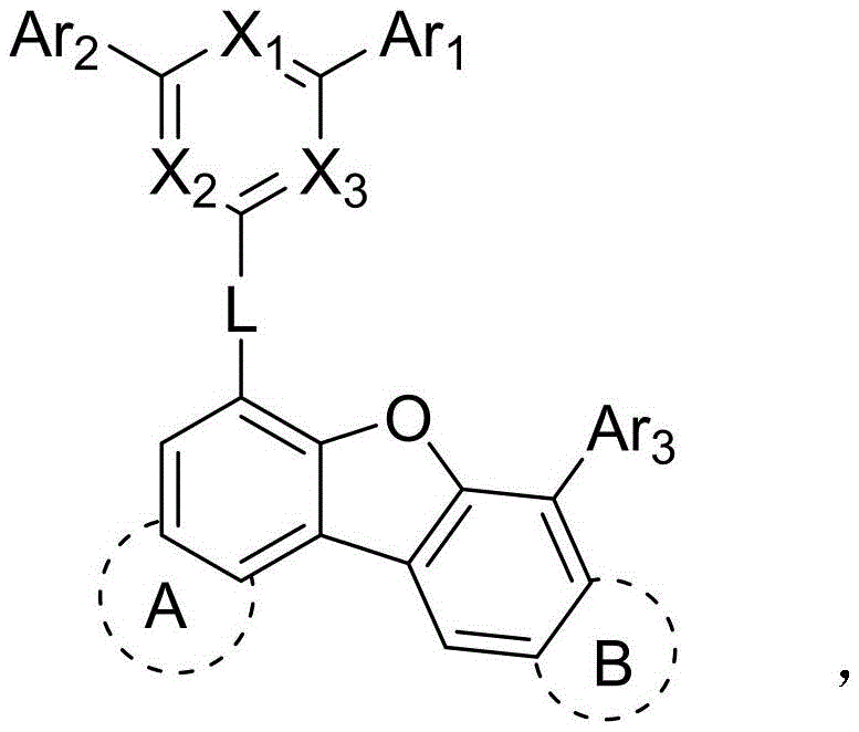
The general structural formula presented in the patent highlights the versatility of the molecular design, where various aryl and heteroaryl substituents can be tuned to optimize energy levels. This modularity allows for precise adjustment of the Lowest Unoccupied Molecular Orbital (LUMO) values, ensuring efficient electron injection from the cathode. For procurement managers and supply chain heads, the significance lies in the fact that these high-performance materials are synthesized via robust, well-established cross-coupling reactions, suggesting a viable path for cost reduction in electronic chemical manufacturing without compromising on the stringent purity specifications required for display applications.
The Limitations of Conventional Methods vs. The Novel Approach
The Limitations of Conventional Methods
Historically, the commercialization of OLED displays has been hindered by the limitations of legacy electron transport materials, most notably Alq3. While Alq3 has served the industry for nearly three decades, its practical application is increasingly restricted by its tendency to migrate into adjacent layers during device operation, leading to instability and reduced lifespan. Furthermore, the electron mobility in many conventional organic materials is generally two to three orders of magnitude lower than hole mobility, creating an imbalance in charge carrier density that necessitates higher driving voltages and generates excess heat. This imbalance not only degrades the organic layers faster but also limits the overall power efficiency of the display panel. Traditional synthesis routes for alternative materials often involve complex multi-step processes with harsh conditions, resulting in low yields and difficult purification challenges that drive up production costs and extend lead times for high-purity electronic chemicals.
The Novel Approach
The novel approach detailed in CN112159397B overcomes these deficiencies by integrating a furan structure with a triazine core, creating a molecule with inherently higher ionization potential and electron affinity. The incorporation of the furan ring, combined with bulky aryl substituents, reduces molecular symmetry and increases conformational isomers, which effectively prevents the molecules from packing too tightly and crystallizing during device operation. This amorphous stability is crucial for maintaining uniform film morphology over thousands of hours of use. Moreover, the synthetic strategy employs a convergent two-step Suzuki coupling protocol, which allows for the modular assembly of the complex architecture from readily available building blocks. This methodological shift not only simplifies the synthesis but also enhances the scalability of the process, making it an attractive option for the commercial scale-up of complex polymer additives and small molecule OLED materials alike.
Mechanistic Insights into Pd-Catalyzed Suzuki Coupling
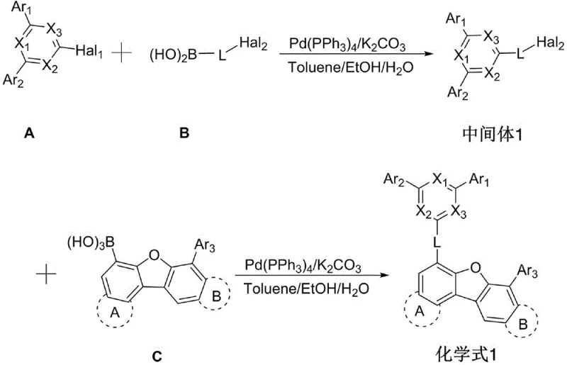
The core of the synthesis strategy relies on the palladium-catalyzed Suzuki-Miyaura cross-coupling reaction, a cornerstone of modern organic synthesis known for its tolerance to functional groups and mild reaction conditions. The mechanism involves the oxidative addition of a palladium(0) species, generated in situ from Pd(PPh3)4, into the carbon-halogen bond of the triazine or aryl halide precursor. This is followed by transmetallation with the organoboron species (boronic acid), facilitated by the base potassium carbonate (K2CO3), which activates the boron center. Finally, reductive elimination releases the coupled product and regenerates the active palladium catalyst. This catalytic cycle is highly efficient, as evidenced by the reaction conditions described in the patent, which utilize a mixed solvent system of toluene, ethanol, and water. The presence of water is particularly advantageous as it aids in the solubility of the inorganic base while maintaining the organic reactants in solution, promoting a homogeneous reaction environment that maximizes conversion rates.
Impurity control is a critical aspect of this mechanistic pathway, especially for electronic grade materials where trace metal contaminants can act as quenching sites for excitons. The patent describes a rigorous workup procedure involving filtration through diatomaceous earth (kieselguhr) to remove the palladium catalyst and inorganic salts immediately after the reaction. Subsequent purification via column chromatography using dichloromethane and petroleum ether ensures the removal of homocoupling byproducts and unreacted starting materials. The result is a material with HPLC purity exceeding 99%, as confirmed by mass spectrometry and elemental analysis in the provided examples. This level of purity is non-negotiable for R&D directors focused on maximizing the external quantum efficiency of the final OLED device, as even ppm-level impurities can drastically reduce device lifetime.
How to Synthesize Furan-Structured Electron Transport Materials Efficiently
The synthesis of these advanced materials is streamlined into a logical two-stage process that balances yield with operational simplicity. The first stage involves the preparation of a key intermediate by coupling a halogenated triazine derivative with an aryl boronic acid. This intermediate is then isolated and purified before undergoing a second coupling reaction with a furan-core boronic acid derivative to form the final target molecule. The detailed standardized synthesis steps outlined below reflect the optimized conditions found in the patent examples, ensuring reproducibility and high quality for pilot and commercial production batches.
- Preparation of Intermediate 1 via Suzuki coupling of halogenated triazine and aryl boronic acid in toluene/ethanol/water.
- Second Suzuki coupling reaction between Intermediate 1 and furan-core boronic acid derivative.
- Purification via column chromatography and recrystallization to achieve >99% HPLC purity.
Commercial Advantages for Procurement and Supply Chain Teams
For procurement managers and supply chain leaders, the transition to this new class of electron transport materials offers substantial strategic benefits beyond mere performance metrics. The reliance on Suzuki coupling means that the supply chain can leverage a vast global network of suppliers for boronic acids and aryl halides, which are commodity chemicals in the pharmaceutical and agrochemical sectors. This abundance of raw materials mitigates the risk of supply disruptions that often plague specialized OLED precursors. Furthermore, the reaction conditions—refluxing in toluene/ethanol/water at moderate temperatures (90-110°C)—are energy-efficient and do not require cryogenic cooling or high-pressure equipment, significantly lowering the capital expenditure (CAPEX) and operational expenditure (OPEX) associated with manufacturing infrastructure.
- Cost Reduction in Manufacturing: The synthetic route eliminates the need for expensive and hazardous reagents often found in older methodologies, such as strong organolithium bases or noble metals other than the recyclable palladium catalyst. The high yields reported in the patent examples, consistently ranging around 86-87% for the final step, indicate excellent atom economy. By minimizing waste and maximizing the output per batch, manufacturers can achieve significant cost savings. Additionally, the straightforward purification process involving standard silica gel chromatography and recrystallization avoids the need for costly preparative HPLC or sublimation steps in the early stages, further driving down the cost of goods sold (COGS).
- Enhanced Supply Chain Reliability: The modular nature of the synthesis allows for flexible production scheduling. Since the intermediate can be stockpiled and reacted with different furan-core derivatives to produce a library of materials (as shown in the patent's extensive list of compounds), manufacturers can respond rapidly to changing customer specifications without retooling the entire production line. This flexibility ensures a continuous supply of high-purity OLED materials, reducing lead times and allowing downstream display manufacturers to maintain their production schedules without interruption. The use of stable, shelf-stable reagents also simplifies inventory management and storage requirements.
- Scalability and Environmental Compliance: The process is inherently scalable from gram-scale laboratory synthesis to multi-ton industrial production. The use of aqueous workups and common organic solvents facilitates waste treatment and solvent recovery, aligning with increasingly stringent environmental regulations. The removal of the palladium catalyst via filtration ensures that the final product meets the strict heavy metal content limits required for consumer electronics. This environmental compliance reduces the regulatory burden on the supply chain and enhances the sustainability profile of the final display product, a key selling point for eco-conscious brands.
Frequently Asked Questions (FAQ)
The following questions address common technical and commercial inquiries regarding the implementation of these furan-structured electron transport materials in OLED manufacturing. These insights are derived directly from the experimental data and technical disclosures within the patent, providing a clear picture of the material's capabilities and processing requirements.
Q: What are the key performance advantages of the furan-structured electron transport materials disclosed in CN112159397B?
A: The materials exhibit higher electron mobility due to the heterocyclic unit's ionization potential and reduced molecular symmetry, which inhibits crystallization and aggregation, thereby extending device lifetime and improving luminous efficiency.
Q: Is the synthesis process scalable for industrial production?
A: Yes, the process utilizes standard Suzuki-Miyaura coupling conditions with commercially available catalysts (Pd(PPh3)4) and bases (K2CO3) in common solvent systems, demonstrating high yields (approx. 86-87%) suitable for scale-up.
Q: How does this material compare to traditional Alq3 electron transport layers?
A: Unlike Alq3, which can migrate to other layers and restrict practical application, these furan-based materials offer superior thermal stability and rigid planar structures that prevent aggregation, ensuring consistent device performance over extended operation.
Partnering with NINGBO INNO PHARMCHEM: Your Reliable Electron Transport Material Supplier
As the demand for high-efficiency, long-lifetime OLED displays continues to surge, partnering with a chemically proficient manufacturer is critical for success. NINGBO INNO PHARMCHEM stands at the forefront of this technological shift, possessing extensive experience scaling diverse pathways from 100 kgs to 100 MT/annual commercial production. Our state-of-the-art facilities are equipped to handle the precise temperature controls and inert atmosphere conditions required for palladium-catalyzed couplings, ensuring that every batch meets stringent purity specifications. With our rigorous QC labs employing HPLC, GC-MS, and ICP-MS for trace metal analysis, we guarantee that our electron transport materials are free from the impurities that compromise device performance.
We invite R&D directors and procurement specialists to collaborate with us to optimize their material supply chains. By leveraging our expertise in process chemistry, we can provide a Customized Cost-Saving Analysis tailored to your specific volume requirements. We encourage you to contact our technical procurement team to request specific COA data and route feasibility assessments for the furan-structured compounds disclosed in CN112159397B. Let us help you accelerate your next-generation display projects with reliable, high-quality materials that deliver on the promise of superior efficiency and durability.