Scaling Novel Spirobifluorene Derivatives for High-Performance OLED Manufacturing
The rapid evolution of the organic light-emitting diode (OLED) industry demands continuous innovation in host and transport materials to achieve higher efficiency and longer operational lifetimes. Patent CN107112439B introduces a significant breakthrough in this domain by disclosing a novel class of spirobifluorene derivatives fused with benzothiophene units. These compounds are specifically engineered to function as hole transport materials within electronic devices, addressing critical limitations found in prior art triarylamine-based systems. The structural integration of benzothiophene moieties into the rigid spirobifluorene backbone results in enhanced thermal stability and superior charge carrier mobility. For procurement specialists and R&D directors seeking a reliable OLED materials supplier, understanding the synthetic accessibility and performance metrics of these derivatives is paramount for next-generation display manufacturing.
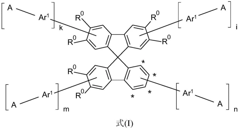
The development of these materials represents a strategic shift towards more robust molecular architectures capable of withstanding the rigorous operating conditions of modern high-brightness displays. By modifying the substitution patterns on the spiro core, the patent demonstrates tunability in energy levels and solubility profiles. This flexibility allows manufacturers to optimize device stacks for specific color emissions, whether blue, green, or red, without compromising the integrity of the hole transport layer. The implications for cost reduction in electronic chemicals manufacturing are substantial, as improved material stability directly correlates with reduced device failure rates and lower warranty claims in the final consumer products.
The Limitations of Conventional Methods vs. The Novel Approach
The Limitations of Conventional Methods
Traditional hole transport materials, such as NPB or MTDATA, often suffer from relatively low glass transition temperatures which can lead to crystallization within the thin film during device operation. This morphological instability creates defects that act as non-radiative recombination centers, drastically reducing the external quantum efficiency and operational lifetime of the OLED. Furthermore, conventional triarylamines may lack sufficient electron blocking capability, allowing electrons to leak through the hole transport layer without recombining with holes in the emissive zone. This imbalance in charge carrier injection necessitates thicker layers or additional blocking layers, complicating the device architecture and increasing the overall production cost. Additionally, the synthesis of some high-performance alternatives often involves complex multi-step routes with poor atom economy, generating significant chemical waste and requiring expensive purification protocols to meet the stringent purity standards of the semiconductor industry.
The Novel Approach
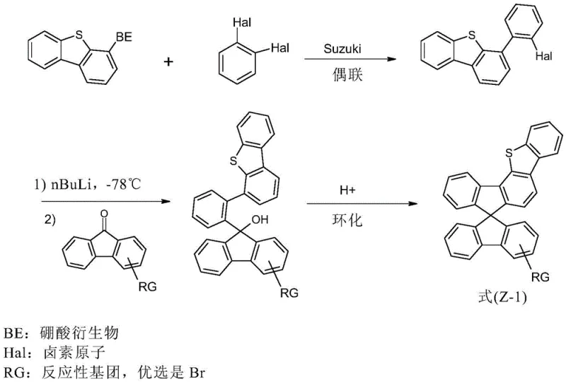
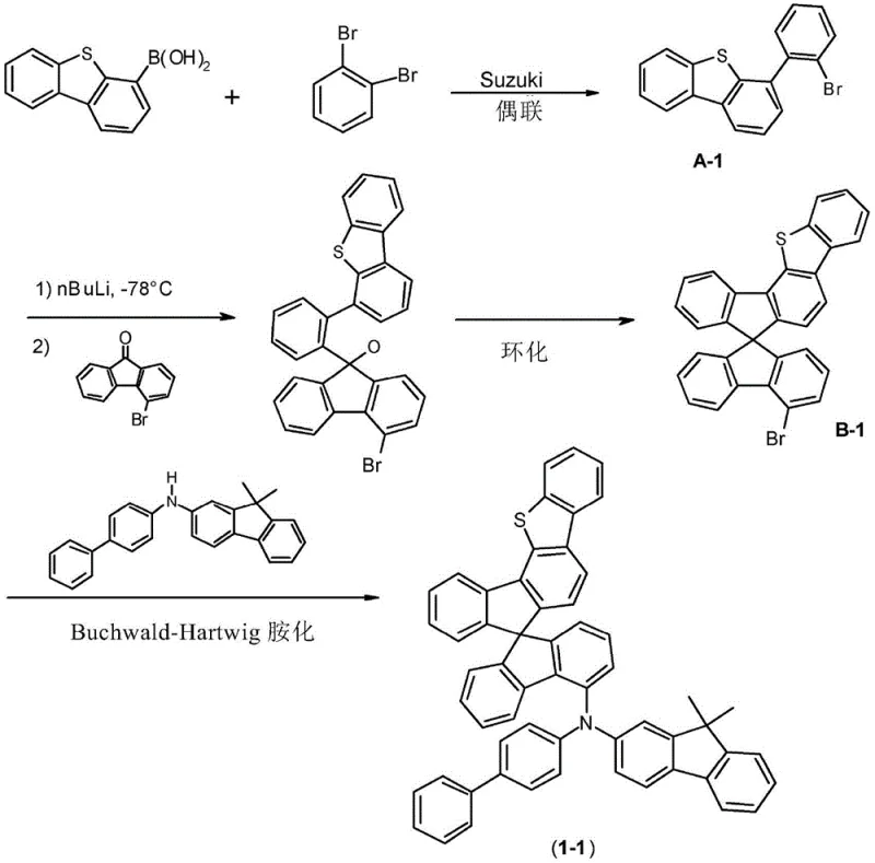
The novel approach detailed in the patent utilizes a fused benzothiophene-spirobifluorene scaffold that inherently possesses a three-dimensional structure, preventing close packing and thus inhibiting crystallization. This amorphous stability is crucial for maintaining uniform film morphology over thousands of hours of operation. The introduction of sulfur-containing heterocycles modifies the electronic distribution, enhancing the hole injection barrier from the anode while simultaneously raising the LUMO level to effectively block electrons. This dual functionality simplifies the device stack by potentially eliminating the need for separate electron blocking layers. From a supply chain perspective, the synthetic route relies on well-established cross-coupling reactions like Suzuki and Buchwald-Hartwig aminations, which are scalable and utilize commercially available starting materials. This ensures that the commercial scale-up of complex organic semiconductors can be achieved with high reproducibility and consistent quality, mitigating supply risks for large panel manufacturers.
Mechanistic Insights into Benzothiophene-Spirobifluorene Cyclization
The core mechanistic advantage of this technology lies in the efficient construction of the spiro junction via an acid-catalyzed cyclization of a tertiary alcohol intermediate. This intermediate is generated through the nucleophilic addition of a lithiated dibenzothiophene derivative to a fluorenone ketone. The reaction proceeds with high regioselectivity, ensuring that the spiro carbon is formed at the desired position to maintain the orthogonality of the pi-systems. This orthogonality is key to preserving the high triplet energy of the material, which prevents back-energy transfer from the emissive dopant to the host matrix. The subsequent functionalization via palladium-catalyzed cross-coupling allows for the precise attachment of bulky diarylamino groups. These groups not only facilitate hole transport through their nitrogen lone pairs but also provide steric bulk that further suppresses intermolecular interactions. For R&D teams, this mechanism offers a versatile platform where the electronic properties can be finely tuned by varying the aryl substituents without altering the core synthetic strategy, enabling rapid iteration and optimization of device performance parameters.
Impurity control is another critical aspect of the mechanistic design, particularly regarding the removal of palladium catalyst residues which can act as quenching sites. The patent outlines purification methods involving silica gel chromatography followed by high-vacuum sublimation. Sublimation is particularly effective for spiro compounds due to their thermal stability and lack of strong intermolecular forces, allowing them to vaporize without decomposition. This process effectively separates the target molecule from higher molecular weight oligomers and residual metal catalysts. The result is a material with extremely low impurity levels, often exceeding 99.9% purity as measured by HPLC. Such high purity is essential for achieving the long lifetimes required in commercial displays, as even trace impurities can accelerate degradation mechanisms under electrical stress. This rigorous purification protocol ensures that the materials delivered to the fabrication line meet the stringent specifications required for high-yield manufacturing.
How to Synthesize Spirobifluorene Derivatives Efficiently
The synthesis of these advanced materials follows a modular approach that begins with the preparation of halogenated dibenzothiophene intermediates. These are coupled with boronic acids or esters to build the necessary biaryl framework before the spiro ring closure. The key to efficiency lies in optimizing the lithiation step, which must be performed at cryogenic temperatures to prevent side reactions, followed by a controlled warming period for the cyclization. Detailed standardized synthesis steps see the guide below. This pathway is designed to maximize yield at each stage while minimizing the formation of difficult-to-remove isomers. For process chemists, understanding the kinetics of the cyclization and the subsequent amination is vital for scaling the reaction from gram to kilogram quantities without losing control over the product profile.
- Perform Suzuki coupling between dibenzothiophene boronic acid and dihalobenzene to form the biaryl intermediate.
- Conduct lithiation of the intermediate at low temperature followed by nucleophilic addition to a fluorenone derivative.
- Execute acid-catalyzed cyclization to close the spiro ring system, followed by purification via chromatography.
- Finalize the structure through Buchwald-Hartwig amination to attach diarylamino groups, ensuring high hole transport capability.
Commercial Advantages for Procurement and Supply Chain Teams
For procurement managers and supply chain heads, the adoption of this patented technology offers several strategic benefits beyond mere performance metrics. The primary advantage is the potential for significant cost optimization through simplified device architectures. By utilizing a material that combines hole transport and electron blocking functions, manufacturers can reduce the total number of deposition steps required per panel. This reduction translates directly into higher throughput and lower capital expenditure on evaporation equipment maintenance. Furthermore, the thermal stability of the spirobifluorene derivatives reduces the risk of material degradation during storage and handling, extending the shelf life of the inventory and reducing waste associated with expired chemicals. The reliance on robust, scalable coupling reactions ensures that the supply chain remains resilient against fluctuations in raw material availability, as the precursors are commodity chemicals produced by multiple global vendors.
- Cost Reduction in Manufacturing: The elimination of separate electron blocking layers and the potential for reduced layer thicknesses due to higher mobility contribute to substantial cost savings. Additionally, the high purity achievable through sublimation reduces the rate of device rejection during quality control testing. By minimizing the occurrence of dark spots or premature failures, the overall yield of the production line improves, effectively lowering the cost per usable unit. The synthetic route avoids the use of extremely expensive or scarce noble metal catalysts in the final steps, relying instead on recyclable palladium systems that are standard in the fine chemical industry, further driving down the bill of materials for the active layers.
- Enhanced Supply Chain Reliability: The synthetic pathway utilizes widely available starting materials such as dibenzothiophene and fluorenone derivatives, which are produced at scale for various industrial applications. This reduces the dependency on single-source suppliers for exotic precursors. The robustness of the Suzuki and Buchwald coupling reactions means that the process is less sensitive to minor variations in reaction conditions, ensuring consistent batch-to-batch quality. This consistency is crucial for maintaining long-term supply agreements with major display panel makers who require guaranteed continuity of supply over multi-year product lifecycles. Reducing lead time for high-purity OLED materials is achieved through streamlined purification workflows that do not require bespoke equipment.
- Scalability and Environmental Compliance: The processes described are amenable to large-scale batch reactors, facilitating the transition from pilot plant to commercial production volumes ranging from hundreds of kilograms to metric tons annually. The use of standard organic solvents allows for established recovery and recycling protocols, aligning with increasingly strict environmental regulations regarding volatile organic compound emissions. The high atom economy of the coupling reactions minimizes the generation of hazardous waste streams. Furthermore, the thermal stability of the final product reduces the energy consumption required for storage and transportation, as strict temperature control is less critical compared to more labile organic semiconductors, contributing to a lower carbon footprint for the logistics network.
Frequently Asked Questions (FAQ)
The following questions address common technical and commercial inquiries regarding the implementation of these spirobifluorene derivatives in OLED manufacturing. The answers are derived directly from the experimental data and embodiments provided in the patent documentation, ensuring accuracy and relevance for technical decision-makers. Understanding these details helps in evaluating the feasibility of integrating these materials into existing production lines and assessing their compatibility with current device stacks.
Q: What performance advantages do benzothiophene-fused spirobifluorenes offer in OLEDs?
A: These derivatives exhibit superior hole transporting properties and electron blocking capabilities compared to conventional triarylamines. The fused benzothiophene unit enhances thermal stability and glass transition temperature, leading to significantly extended device lifetime and improved quantum efficiency in both fluorescent and phosphorescent OLED architectures.
Q: How is high purity achieved for these electronic chemicals?
A: The synthesis protocol incorporates rigorous purification stages, including silica gel chromatography to remove catalyst residues and by-products. Crucially, the final compounds undergo high-vacuum sublimation, a standard in the display industry, to achieve purity levels exceeding 99.9% as verified by HPLC, ensuring minimal impurity-induced quenching in the emissive layer.
Q: Are these materials compatible with solution processing techniques?
A: Yes, the patent specifies that suitable substitution patterns on the spirobifluorene core can enhance solubility in organic solvents such as toluene and chlorobenzene. This makes the materials viable for inkjet printing and spin-coating applications, offering flexibility for manufacturers transitioning from thermal evaporation to lower-cost solution-based manufacturing processes.
Partnering with NINGBO INNO PHARMCHEM: Your Reliable Spirobifluorene Derivatives Supplier
The technological potential of benzothiophene-fused spirobifluorenes is immense, offering a pathway to OLEDs with superior lifetime and efficiency characteristics. NINGBO INNO PHARMCHEM stands ready to support your development efforts as a seasoned CDMO partner with extensive experience scaling diverse pathways from 100 kgs to 100 MT/annual commercial production. Our facilities are equipped with state-of-the-art purification suites capable of meeting stringent purity specifications required for electronic grade materials. With rigorous QC labs employing HPLC, GC-MS, and ICP-MS for trace metal analysis, we ensure that every batch delivered meets the exacting standards of the display industry. We understand the critical nature of supply continuity and have established robust raw material sourcing networks to mitigate disruption risks.
We invite you to initiate a dialogue regarding your specific material requirements and supply chain optimization goals. Our technical procurement team is prepared to provide a Customized Cost-Saving Analysis tailored to your current bill of materials. By collaborating with us, you can access specific COA data and route feasibility assessments that will clarify the path from laboratory curiosity to commercial reality. Let us help you secure a competitive advantage through advanced material science and reliable manufacturing execution.
Engineering Bottleneck?
Can't scale up this synthesis? Upload your target structure or CAS, and our CDMO team will evaluate the industrial feasibility within 24 hours. Request Evaluation →