Advanced Binaphthyl-Based Hole Transport Materials for Next-Gen OLED and Solar Applications
The rapid evolution of the optoelectronic industry demands materials that can withstand rigorous operational conditions while maintaining high efficiency. Traditional hole transport materials (HTMs) like TPD and NPB have long served the industry, yet their inherent limitations in thermal stability often lead to device degradation. Addressing this critical bottleneck, Patent CN111233676A introduces a groundbreaking class of organic small molecule hole transport materials characterized by a unique binaphthyl core structure. This innovation represents a significant leap forward for manufacturers seeking reliable OLED material solutions that combine high glass transition temperatures with optimized HOMO energy levels. By strategically integrating rigid aromatic units, this technology ensures superior morphological stability, directly translating to extended device lifetimes and enhanced performance in both display and photovoltaic applications.
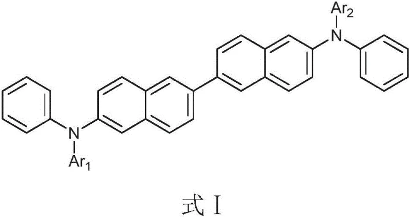
The strategic design of these molecules leverages the rigidity of the 2,2'-binaphthyl bridge to prevent molecular rotation and aggregation, which are primary causes of film instability in organic electronics. Unlike conventional linear structures, this architecture supports strong pi-pi stacking interactions that facilitate efficient charge carrier mobility without compromising thermal integrity. For R&D teams focused on next-generation displays, this material offers a robust platform for developing devices that operate at lower voltages with higher luminous efficiency. The versatility of the structure allows for further fine-tuning through various end-group substitutions, making it a highly adaptable candidate for a wide range of electronic chemical manufacturing processes.
The Limitations of Conventional Methods vs. The Novel Approach
The Limitations of Conventional Methods
Historically, the industry has relied heavily on materials such as TPD, TAPC, and NPB for hole transport layers. However, these legacy compounds suffer from critically low glass transition temperatures, typically ranging from 58°C to 98°C. In high-brightness OLED operations, the heat generated can easily exceed these thresholds, causing the amorphous film to crystallize. This crystallization creates defects that act as non-radiative recombination centers, drastically reducing device efficiency and leading to premature failure. Furthermore, in the realm of perovskite solar cells, expensive materials like spiro-OMeTAD are often required to achieve high performance, creating a significant barrier to commercial scalability. The reliance on such costly and thermally unstable components restricts the ability of supply chains to deliver consistent, high-volume production runs necessary for mass-market adoption.
The Novel Approach
The methodology outlined in the patent overcomes these challenges by employing a modular synthetic strategy centered on the binaphthyl scaffold. By coupling electron-rich aromatic amines with rigid end groups such as fluorene, carbazole, dibenzofuran, or dibenzothiophene, the resulting compounds exhibit glass transition temperatures exceeding 140°C. This substantial increase in thermal stability ensures that the thin films remain amorphous and uniform even under prolonged thermal stress. Additionally, the electronic properties of the end groups effectively deepen the HOMO energy level, facilitating better energy alignment with adjacent layers. This dual improvement in thermal and electronic properties positions this new class of materials as a superior alternative for cost reduction in electronic chemical manufacturing, enabling the production of more durable and efficient optoelectronic devices.
Mechanistic Insights into Binaphthyl-Core Rigidity and Charge Transport
The exceptional performance of these materials stems from the synergistic interaction between the central binaphthyl unit and the terminal aromatic substituents. The binaphthyl core acts as a rigid spacer that inhibits intramolecular rotation, thereby increasing the activation energy required for structural relaxation. This rigidity is crucial for maintaining the amorphous state of the film, which is essential for uniform charge transport. Simultaneously, the terminal groups, such as the 9,9-dimethylfluorene or 9-methylcarbazole units, provide extensive conjugation pathways that enhance hole mobility. The electron-donating nature of the nitrogen atoms in the amine linkages further enriches the electron density across the molecule, lowering the ionization potential. This mechanistic design ensures that holes can be injected and transported with minimal resistance, directly contributing to the lowered operating voltage observed in devices utilizing these materials.
Impurity control is another critical aspect of the synthesis mechanism that ensures high purity for commercial applications. The synthetic route employs specific catalytic systems, such as CuI/1,10-phenanthroline for C-N bond formation and Pd(PPh3)4 for C-C coupling, which are known for their high selectivity. The purification protocols described involve precise recrystallization and column chromatography steps using solvent systems like petroleum ether and dichloromethane. These methods effectively remove unreacted starting materials and catalyst residues, which are common sources of device quenching. By strictly controlling the stoichiometry and reaction conditions, such as maintaining temperatures between 115°C and 190°C depending on the step, the process minimizes side reactions. This rigorous approach to synthesis guarantees a clean impurity profile, which is vital for achieving the stringent quality standards required by top-tier display manufacturers.
How to Synthesize High-Performance Hole Transport Materials Efficiently
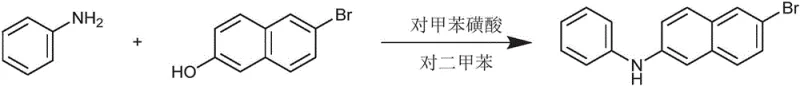
The preparation of these advanced materials follows a logical, four-step sequence that balances chemical complexity with operational feasibility. The process begins with the formation of a key naphthylamine intermediate, followed by sequential functionalization to attach the rigid end groups. Each step is optimized for high yield and scalability, utilizing standard organic synthesis techniques that are easily transferable to pilot and production scales. The use of commercially available catalysts and solvents further simplifies the logistical requirements for manufacturing. Detailed below is the standardized workflow that enables the efficient production of these high-value intermediates, ensuring consistency and reproducibility across different batches.
- Step 1: Acid-catalyzed reaction of 6-bromo-2-naphthol with aniline in xylene at 150-210°C to form 6-bromo-N-phenyl-2-naphthylamine.
- Step 2: Copper-catalyzed Ullmann-type coupling of the intermediate with aryl iodides (fluorene or carbazole derivatives) using CuI and ligands.
- Step 3: Palladium-catalyzed borylation of the bromo-intermediate using bis(pinacolato)diboron to generate the boronic ester precursor.
- Step 4: Final Suzuki-Miyaura cross-coupling between the bromo-intermediate and the boronic ester using Pd(PPh3)4 to yield the target dimer.
Commercial Advantages for Procurement and Supply Chain Teams
From a procurement perspective, the adoption of this synthetic route offers transformative benefits regarding cost structure and supply security. The reliance on commodity chemicals such as aniline, naphthol, and simple halogenated aromatics means that raw material sourcing is stable and unaffected by the volatility associated with exotic precursors. The elimination of complex, multi-step protection and de-protection sequences further streamlines the production timeline. This simplicity translates directly into reduced operational expenditures, allowing manufacturers to offer competitive pricing without sacrificing quality. For supply chain leaders, the robustness of this chemistry ensures that production schedules can be met reliably, mitigating the risks of delays that often plague the sourcing of specialized electronic materials.
- Cost Reduction in Manufacturing: The synthetic pathway avoids the use of prohibitively expensive catalysts or rare earth metals, relying instead on established copper and palladium systems that are cost-effective at scale. The high yields reported in the patent examples, often exceeding 85% for key coupling steps, minimize waste and maximize material throughput. Additionally, the purification methods utilize standard solvents and techniques, avoiding the need for specialized equipment or hazardous reagents. This efficiency drives down the cost per kilogram significantly, making high-performance HTMs accessible for mass-market applications like large-area lighting and consumer electronics.
- Enhanced Supply Chain Reliability: The starting materials for this synthesis are widely produced bulk chemicals with established global supply networks. This reduces dependency on single-source suppliers for niche intermediates, thereby enhancing supply chain resilience. The robustness of the reaction conditions, which tolerate standard protective atmospheres like nitrogen or argon without requiring extreme pressures or cryogenic temperatures, further simplifies facility requirements. Consequently, multiple contract manufacturing organizations (CMOs) can potentially qualify to produce these materials, creating a diversified supply base that safeguards against disruptions.
- Scalability and Environmental Compliance: The process is inherently scalable, as demonstrated by the successful execution of reactions on gram scales with consistent results. The waste streams generated are primarily organic solvents which can be recovered and recycled using standard distillation units, aligning with modern green chemistry principles. The absence of heavy metal contaminants in the final product, due to effective purification, reduces the environmental burden associated with disposal. This compliance with environmental standards facilitates smoother regulatory approvals and supports the sustainability goals of downstream device manufacturers.
Frequently Asked Questions (FAQ)
The following questions address common technical and commercial inquiries regarding the implementation of this technology. These insights are derived directly from the experimental data and structural analysis provided in the patent documentation. Understanding these aspects is crucial for technical teams evaluating the feasibility of integrating these materials into existing production lines.
Q: How does the binaphthyl core improve thermal stability compared to traditional TPD?
A: The introduction of a rigid binaphthyl bridge combined with bulky end groups like fluorene or carbazole significantly increases molecular rigidity. This structural enhancement raises the glass transition temperature (Tg) to over 140°C, compared to ~58°C for TPD, preventing crystallization and extending OLED device lifespan.
Q: What are the cost advantages of this synthesis route?
A: The synthesis utilizes inexpensive commodity chemicals such as aniline and naphthol derivatives. Furthermore, the avoidance of complex multi-step functionalizations and the use of robust catalytic systems (CuI/Pd) allow for high yields and simplified purification, drastically reducing overall manufacturing costs.
Q: Can this material be used in perovskite solar cells?
A: Yes, the material features a deepened HOMO energy level due to the electron-donating end groups, which facilitates efficient hole extraction. This makes it highly suitable not only for OLEDs but also for high-efficiency perovskite and organic solar cell applications.
Partnering with NINGBO INNO PHARMCHEM: Your Reliable Hole Transport Material Supplier
At NINGBO INNO PHARMCHEM, we recognize the critical role that advanced hole transport materials play in the future of optoelectronics. Our team possesses extensive experience scaling diverse pathways from 100 kgs to 100 MT/annual commercial production, ensuring that your transition from lab-scale discovery to industrial application is seamless. We adhere to stringent purity specifications and operate rigorous QC labs to guarantee that every batch meets the exacting standards required for high-end OLED and solar cell fabrication. Our commitment to quality ensures that the thermal and electronic properties of the materials are preserved throughout the manufacturing process.
We invite you to collaborate with us to optimize your supply chain and reduce your overall material costs. Our technical procurement team is ready to provide a Customized Cost-Saving Analysis tailored to your specific volume requirements. Contact us today to request specific COA data and route feasibility assessments, and let us demonstrate how our expertise can accelerate your product development cycle.
Engineering Bottleneck?
Can't scale up this synthesis? Upload your target structure or CAS, and our CDMO team will evaluate the industrial feasibility within 24 hours. Request Evaluation →