Advanced Organic Electroluminescent Compounds for High-Performance OLED Display Manufacturing
The rapid evolution of the organic light-emitting diode (OLED) industry demands materials that surpass the limitations of legacy technologies in terms of efficiency, stability, and power consumption. Patent CN112079834A introduces a groundbreaking class of organic electroluminescent compounds defined by a unique spiro-bridged structural framework, designated as Formula I. These compounds are specifically engineered to function as superior hole transport materials within the organic layers of electroluminescent devices. Unlike conventional linear amines, the three-dimensional rigidity of this core structure inhibits crystallization and enhances thermal stability, which are critical factors for the longevity of commercial displays. The general structural formula encompasses a diverse range of substituents, allowing for fine-tuning of HOMO/LUMO energy levels to match various emissive layers. 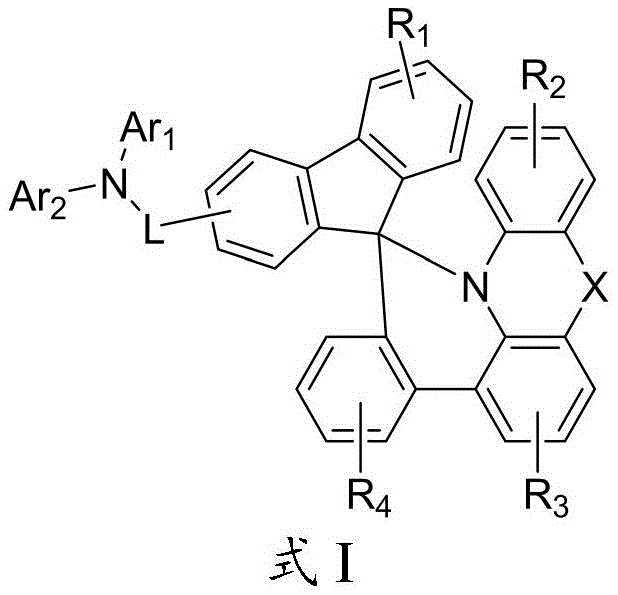
For procurement specialists and supply chain managers evaluating a reliable OLED material supplier, the versatility of Formula I offers a strategic advantage. The ability to modify Ar1, Ar2, and the bridging atom X means that a single synthetic platform can generate a library of materials tailored for specific blue, green, or red phosphorescent hosts. This modularity reduces the risk associated with sourcing single-point failure materials. Furthermore, the patent explicitly highlights that devices fabricated with these compounds exhibit excellent current efficiency and power efficiency alongside a prolonged service life. This technical breakthrough addresses the persistent industry challenge of balancing high brightness with operational stability, making these compounds highly attractive for next-generation smartphone and television panel manufacturing.
The Limitations of Conventional Methods vs. The Novel Approach
The Limitations of Conventional Methods
Historically, the hole transport layer (HTL) in OLED devices has relied heavily on materials such as N,N'-di(1-naphthyl)-N,N'-diphenyl-(1,1'-biphenyl)-4,4'-diamine (NPB) or copper phthalocyanine (CuPc). While these materials established the foundation of the industry, they suffer from inherent drawbacks that limit the performance ceiling of modern high-resolution displays. NPB, for instance, has a relatively low glass transition temperature, which leads to morphological instability under the heat generated during prolonged operation. This instability causes phase separation and crystallization within the thin film, creating non-radiative recombination centers that degrade luminance efficiency over time. 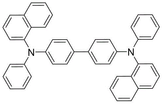
Moreover, devices utilizing these traditional HTL materials often require higher driving voltages to achieve standard brightness levels, such as 5000 cd/m². Higher voltage operation not only increases power consumption—a critical metric for battery-powered mobile devices—but also accelerates the degradation of the organic layers. The quantum efficiency of legacy materials often plateaus, failing to meet the stringent requirements for ultra-high-definition and flexible display applications. Consequently, there is an urgent technical imperative to replace these linear, flexible amine structures with more robust, three-dimensional architectures that can withstand the rigors of commercial device operation without sacrificing charge transport mobility.
The Novel Approach
The novel approach detailed in the patent leverages a spiro-fluorene or spiro-acridine fused core that fundamentally alters the physical properties of the hole transport material. By introducing a orthogonal spiro-connection, the molecule achieves a bulky, non-planar geometry that effectively suppresses intermolecular aggregation and crystallization. This structural rigidity translates directly into enhanced thermal stability and a higher glass transition temperature, ensuring that the morphology of the hole transport layer remains intact even under thermal stress. The patent data demonstrates that devices incorporating these new compounds achieve significantly lower driving voltages compared to NPB-based controls. For example, while NPB devices may require 5.2V to reach 5000 cd/m², the new compounds can achieve the same brightness at voltages as low as 3.1V to 3.8V.
Beyond voltage reduction, the novel compounds exhibit a dramatic improvement in operational lifetime. The patent reports T95 lifetimes exceeding 250 hours for the new materials, compared to merely 68.9 hours for NPB under identical testing conditions. This nearly four-fold increase in stability is a game-changer for display manufacturers aiming to guarantee product longevity. The synthetic design also allows for the incorporation of electron-withdrawing or electron-donating groups to precisely tune the ionization potential, facilitating better energy level alignment with the adjacent emissive layer. This optimization minimizes the energy barrier for hole injection, thereby improving the overall quantum efficiency of the device and reducing the likelihood of exciton quenching at the interfaces.
Mechanistic Insights into the Spiro-Core Construction and Functionalization
The synthesis of these high-performance materials relies on a sophisticated yet scalable three-step sequence that constructs the complex spiro-scaffold before functionalizing it with charge-transporting amine groups. The process begins with a cryogenic lithiation step, where a bromo-substituted precursor is treated with n-butyllithium at -78°C. This generates a highly reactive organolithium species which then undergoes nucleophilic addition to a ketone substrate, typically a fluorenone derivative. This step is critical for establishing the quaternary carbon center that defines the spiro-junction. The reaction is quenched carefully to yield a hydroxy-intermediate, which serves as the precursor for the ring-closing reaction. The precision required in temperature control during this stage ensures high regioselectivity and minimizes side reactions that could compromise the purity of the final electronic material.
Following the formation of the hydroxy-intermediate, the synthesis proceeds to an acid-catalyzed cyclization. This step utilizes concentrated sulfuric acid in glacial acetic acid at elevated temperatures (around 80°C) to dehydrate the alcohol and close the ring, forming the rigid spiro-fused core. This transformation is the key to unlocking the thermal stability benefits of the material. Finally, the core is functionalized via palladium-catalyzed cross-coupling reactions, such as Buchwald-Hartwig amination or Suzuki coupling. 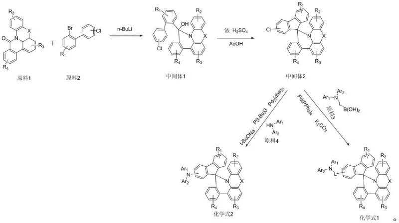
In the final coupling stage, the chloro-substituted spiro-intermediate reacts with various aryl amines or boronic acids in the presence of a palladium catalyst and a base. This step allows for the modular attachment of the Ar1 and Ar2 groups described in Formula I. The use of robust catalysts like Pd2(dba)3 with bulky phosphine ligands ensures that even sterically hindered amines can be coupled efficiently. This mechanistic pathway is advantageous for cost reduction in electronic chemical manufacturing because it avoids the use of expensive noble metal catalysts in the early stages and reserves the palladium catalysis for the final, high-value functionalization step. The result is a highly pure product with a well-defined impurity profile, essential for preventing dark spots in OLED panels.
How to Synthesize High-Purity Organic Electroluminescent Compounds Efficiently
The preparation of these compounds follows a logical progression from simple commercially available starting materials to the complex final architecture. The process is designed to maximize yield at each stage while maintaining the stringent purity levels required for electronic grade materials. The initial lithiation and addition steps build the carbon skeleton, while the subsequent acid treatment locks the conformation. The final coupling step introduces the electronic functionality. Detailed standard operating procedures for each reaction condition, including stoichiometry and workup protocols, are essential for reproducibility.
- Perform cryogenic lithiation of the bromo-precursor at -78°C followed by nucleophilic addition to the ketone substrate to form the hydroxy-intermediate.
- Execute acid-catalyzed cyclization using concentrated sulfuric acid in glacial acetic acid at 80°C to construct the rigid spiro-core scaffold.
- Conduct palladium-catalyzed cross-coupling (Buchwald-Hartwig or Suzuki) at elevated temperatures (95-110°C) to attach the amine or aryl substituents.
Commercial Advantages for Procurement and Supply Chain Teams
From a supply chain perspective, the adoption of this synthetic route offers distinct advantages over more convoluted methods often seen in academic literature. The reliance on commodity chemicals such as tetrahydrofuran, acetic acid, and standard palladium catalysts means that the raw material supply chain is robust and less susceptible to geopolitical disruptions. The synthetic route is concise, typically requiring only three main isolation steps to reach the final product. This brevity is a significant driver for cost reduction in display material manufacturing, as fewer unit operations translate to lower labor costs, reduced solvent consumption, and higher overall throughput in a production facility. The high yields reported in the patent examples, often exceeding 70-80% for individual steps, further contribute to a favorable cost of goods sold (COGS).
- Cost Reduction in Manufacturing: The elimination of exotic reagents and the use of standard industrial solvents significantly lowers the direct material costs. Furthermore, the high efficiency of the palladium-catalyzed coupling step minimizes the loss of valuable amine precursors. By avoiding multi-step protection and deprotection strategies common in other complex organic syntheses, the process reduces waste generation and simplifies the purification workflow. This streamlined approach allows for substantial cost savings when scaling from laboratory grams to commercial metric tons, making high-performance OLED materials more economically viable for mass-market electronics.
- Enhanced Supply Chain Reliability: The starting materials, such as bromo-biphenyls and fluorenones, are widely produced by the bulk chemical industry, ensuring a stable supply base. The synthetic protocol does not rely on custom-synthesized intermediates that might have long lead times. This accessibility reduces the risk of production delays and allows for better inventory management. For a reliable OLED material supplier, this means the ability to guarantee consistent delivery schedules to panel manufacturers, even during periods of high demand. The robustness of the chemistry also means that technology transfer to different manufacturing sites can be achieved with minimal friction.
- Scalability and Environmental Compliance: The process conditions, while requiring careful temperature control, are well within the capabilities of standard stainless steel reactors found in fine chemical plants. The absence of extremely hazardous reagents simplifies safety management and waste treatment protocols. The workup procedures involve standard extractions and crystallizations, which are easily scalable. This ease of scale-up supports the commercial scale-up of complex organic semiconductors without requiring massive capital expenditure on specialized equipment. Additionally, the high atom economy of the coupling reactions aligns with modern green chemistry principles, reducing the environmental footprint of the manufacturing process.
Frequently Asked Questions (FAQ)
The following questions address common technical and commercial inquiries regarding the implementation of these new electroluminescent compounds in industrial settings. Understanding the nuances of the material's performance and synthesis helps stakeholders make informed decisions about integrating this technology into their product roadmaps.
Q: How does this new compound class improve OLED device lifetime compared to traditional materials like NPB?
A: The patented compounds feature a rigid spiro-bridged backbone that enhances thermal stability and morphological stability, resulting in significantly extended operational lifetimes (T95) compared to conventional NPB layers.
Q: What are the key driving voltage advantages of these electroluminescent materials?
A: Devices utilizing these materials demonstrate markedly lower driving voltages (e.g., 3.8V vs 5.2V for NPB at 5000 cd/m²), which directly translates to reduced power consumption and improved energy efficiency in display panels.
Q: Is the synthetic route scalable for industrial production of these OLED intermediates?
A: Yes, the synthesis utilizes standard industrial reagents and avoids exotic catalysts. The three-step process yields high purity products with robust yields suitable for commercial scale-up from kilograms to metric tons.
Partnering with NINGBO INNO PHARMCHEM: Your Reliable Organic Electroluminescent Compound Supplier
The technical potential of the compounds described in Patent CN112079834A represents a significant leap forward in OLED material science, offering a pathway to brighter, more efficient, and longer-lasting displays. At NINGBO INNO PHARMCHEM, we possess extensive experience scaling diverse pathways from 100 kgs to 100 MT/annual commercial production, ensuring that promising laboratory discoveries are successfully translated into industrial reality. Our facilities are equipped with rigorous QC labs capable of meeting the stringent purity specifications required for electronic grade materials, including the detection of trace metal impurities that could degrade device performance. We understand that the transition from prototype to mass production requires a partner who can navigate the complexities of process optimization and regulatory compliance.
We invite display manufacturers and material integrators to collaborate with us on optimizing the supply chain for these advanced hole transport materials. Our technical team is ready to provide a Customized Cost-Saving Analysis tailored to your specific volume requirements and device architecture. By leveraging our expertise in process chemistry and scale-up engineering, we can help you reduce lead time for high-purity electroluminescent compounds and secure a competitive advantage in the marketplace. Please contact our technical procurement team to request specific COA data and route feasibility assessments for your next-generation OLED projects.
Engineering Bottleneck?
Can't scale up this synthesis? Upload your target structure or CAS, and our CDMO team will evaluate the industrial feasibility within 24 hours. Request Evaluation →