Revolutionizing Blue OLED Efficiency with Advanced Bipolar Organic Semiconductor Materials
The landscape of organic optoelectronics is undergoing a significant transformation, driven by the urgent demand for stable and efficient blue light emitters in next-generation display technologies. Patent CN103450190A introduces a groundbreaking organic semiconductor material that strategically integrates triphenylamine, carboline, and benzene anthracene moieties into a single molecular architecture. This innovative design addresses the longstanding bottleneck in the industry regarding the lack of host materials that possess both high triplet energy levels and balanced carrier transport properties. By functioning as a bipolar blue light material, this compound eliminates the need for complex doping strategies often required with traditional unipolar hosts, thereby simplifying the device architecture. For R&D directors and procurement specialists, this represents a pivotal shift towards materials that offer not only superior electroluminescent efficiency but also enhanced manufacturability and supply chain resilience in the competitive display market.
The Limitations of Conventional Methods vs. The Novel Approach
The Limitations of Conventional Methods
Historically, the development of high-efficiency organic light-emitting diodes (OLEDs), particularly in the blue spectrum, has been hindered by the reliance on organo-metallic phosphorescent substances. While these materials can theoretically achieve 100% internal quantum efficiency by harvesting both singlet and triplet excitons, they suffer from significant practical drawbacks. The excited state exciton lifespan of transition metal complexes is relatively long, which frequently leads to unwanted triplet-triplet annihilation during actual device operation, causing efficiency roll-off at high brightness levels. Furthermore, the scarcity and high cost of precious metals like iridium and platinum create substantial supply chain vulnerabilities and inflate the bill of materials for mass production. These conventional methods often require intricate device engineering to mitigate stability issues, resulting in increased fabrication complexity and reduced overall yield rates for manufacturers aiming for large-area flat-panel displays.
The Novel Approach
In stark contrast, the novel approach detailed in the patent leverages a purely organic molecular design that intrinsically balances hole and electron transport capabilities without relying on scarce heavy metals. By incorporating triphenylamine units known for their excellent hole transport properties and carboline units recognized for their electron transport performance, the material achieves a natural charge balance within the emissive layer. The inclusion of benzene anthracene further enhances the fluorescence quantum yield, ensuring bright and pure blue emission. This structural innovation allows for the creation of electroluminescent devices that are not only highly efficient but also thermally robust, with decomposition temperatures exceeding 470°C. This shift from metal-dependent phosphorescence to organic bipolar fluorescence offers a pathway to drastically simplified manufacturing processes and significantly reduced raw material costs, making it an attractive option for cost-sensitive consumer electronics applications.
Mechanistic Insights into Acid-Catalyzed Condensation and Suzuki Coupling
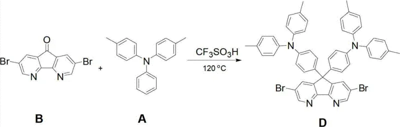
The synthesis of the key intermediate, Compound D, involves a sophisticated acid-catalyzed condensation reaction that forms the rigid carboline core essential for the material's thermal stability. In this step, 3,6-dibromo-1,8-phenanthroline-9-one reacts with 4,4'-dimethyltriphenylamine under an inert nitrogen atmosphere at elevated temperatures ranging from 110°C to 120°C. The use of trifluoromethanesulfonic acid as a catalyst facilitates the formation of the carbon-carbon bonds necessary to fuse the aromatic systems, resulting in a high crude yield of approximately 91%. This high conversion rate is critical for minimizing waste and maximizing the throughput of the initial synthesis stage. The rigorous control of reaction conditions, including the precise molar ratios and the exclusion of oxygen, ensures that the resulting intermediate possesses the structural integrity required for subsequent functionalization, laying the foundation for the high purity of the final semiconductor material.
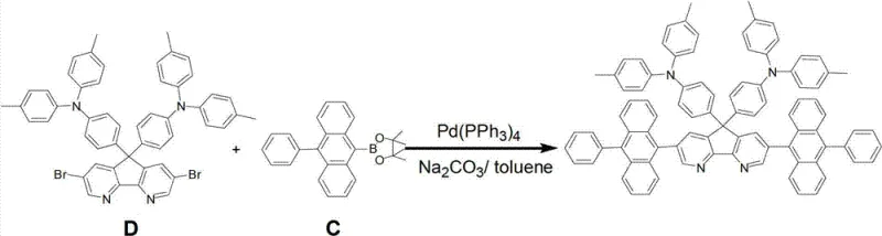
Following the formation of the intermediate, the final assembly of the organic semiconductor is achieved through a palladium-catalyzed Suzuki-Miyaura cross-coupling reaction. This versatile and robust chemical transformation links the brominated carboline intermediate with 10-phenylanthracene-9-boronic acid pinacol ester. The reaction proceeds efficiently in organic solvents such as toluene or DMF, utilizing bases like sodium carbonate or potassium carbonate to activate the boronic ester. The patent highlights the flexibility of this step, demonstrating successful coupling with various palladium catalyst systems, including tetrakis(triphenylphosphine)palladium(0) and tris(dibenzylideneacetone)dipalladium(0) with S-phos ligands. This adaptability allows manufacturers to optimize catalyst loading and reaction times, typically ranging from 10 to 30 hours, to suit their specific production scales while maintaining yields between 74% and 80%. The resulting molecule exhibits a maximum emission peak around 447nm, confirming its suitability as a high-performance blue light emitter.
How to Synthesize 3,6-bis-(10-benzene anthracene-9-yl)-9,9-bis-(4-(di-p-tolylamino)phenyl)-1,8-carboline Efficiently
The efficient synthesis of this high-value organic semiconductor requires strict adherence to the optimized two-step protocol outlined in the patent data to ensure reproducibility and high purity. The process begins with the preparation of the brominated carboline precursor, followed by the critical cross-coupling step that installs the anthracene units responsible for the blue emission characteristics. Operators must maintain an inert atmosphere throughout to prevent oxidation of the sensitive intermediates and catalysts. Detailed standardized synthesis steps, including specific reagent grades, solvent drying procedures, and purification protocols via silica gel column chromatography, are essential for achieving the electronic-grade quality required for OLED applications. The following guide provides the structured framework for executing this synthesis in a controlled laboratory or pilot plant environment.
- Synthesize the carboline intermediate (Compound D) via condensation of dibromo-phenanthroline-fluorenone and dimethyltriphenylamine using trifluoromethanesulfonic acid.
- Perform Suzuki-Miyaura coupling between the brominated intermediate and phenylanthracene boronic ester using palladium catalysts.
- Purify the crude product through solvent extraction, drying, and silica gel column chromatography to achieve electronic-grade purity.
Commercial Advantages for Procurement and Supply Chain Teams
From a strategic procurement perspective, the adoption of this organic semiconductor material offers compelling advantages over traditional metal-complex-based emitters. The primary driver for cost optimization lies in the elimination of expensive and supply-constrained precious metals such as iridium and platinum from the bill of materials. By utilizing abundant organic feedstocks and standard palladium catalysts which can often be recovered or used in lower loadings, the raw material costs are significantly reduced. Furthermore, the high thermal stability of the material reduces the risk of degradation during storage and handling, minimizing inventory losses. The synthesis route relies on well-established chemical transformations like Suzuki coupling, which are widely understood and easily scalable by contract development and manufacturing organizations (CDMOs), ensuring a reliable and diversified supply base for global electronics manufacturers seeking to mitigate supply chain risks.
- Cost Reduction in Manufacturing: The transition to this all-organic bipolar material fundamentally alters the cost structure of OLED production by removing the dependency on volatile precious metal markets. The synthetic route utilizes commodity chemicals and avoids the need for specialized metallo-organic precursors that command premium pricing. Additionally, the high yields reported in the patent examples indicate a material-efficient process that minimizes solvent usage and waste disposal costs associated with low-yielding reactions. This cumulative effect results in substantial cost savings per kilogram of active material produced, allowing display manufacturers to improve their margins or pass savings on to consumers in a highly competitive market.
- Enhanced Supply Chain Reliability: Supply chain continuity is bolstered by the use of chemically stable intermediates and reagents that are commercially available from multiple global suppliers. Unlike custom-synthesized metal complexes that may have single-source bottlenecks, the building blocks for this organic semiconductor, such as triphenylamine derivatives and boronic esters, are part of the standard inventory for many fine chemical producers. This redundancy in the supply base ensures that production schedules are not disrupted by raw material shortages. Moreover, the robustness of the synthesis allows for flexible manufacturing locations, enabling regional production hubs to serve local display fabs and reduce logistics lead times.
- Scalability and Environmental Compliance: The scalability of this process is evidenced by the use of standard reflux conditions and common organic solvents like toluene and THF, which are compatible with existing large-scale reactor infrastructure. The purification steps involve standard workup procedures such as aqueous extraction and column chromatography, which can be adapted for continuous processing or large batch operations. From an environmental standpoint, the avoidance of heavy metal waste streams simplifies effluent treatment and regulatory compliance. The high thermal stability of the final product also contributes to energy efficiency during the device fabrication process, as it can withstand higher processing temperatures without decomposition, aligning with green manufacturing initiatives.
Frequently Asked Questions (FAQ)
The following questions address common technical and commercial inquiries regarding the implementation of this organic semiconductor technology in industrial settings. These answers are derived directly from the experimental data and beneficial effects described in the patent documentation, providing clarity on performance metrics and process capabilities. Understanding these details is crucial for technical teams evaluating the material for integration into existing display manufacturing lines or for developing new device architectures that leverage the unique bipolar transport properties of this compound.
Q: Why is this bipolar material superior for blue OLEDs compared to traditional phosphorescent dopants?
A: Traditional phosphorescent dopants often rely on scarce transition metals like iridium, which can suffer from triplet-triplet annihilation and stability issues. This organic semiconductor utilizes a bipolar design combining triphenylamine and carboline units, offering balanced charge transport and high triplet energy levels without the instability associated with metal complexes, leading to longer device lifetimes and consistent blue emission.
Q: What are the scalability advantages of the Suzuki coupling method used in this patent?
A: The Suzuki-Miyaura coupling employed here uses widely available palladium catalysts and boronic acid derivatives, which are standard in industrial fine chemical manufacturing. Unlike specialized vacuum deposition processes required for some small molecules, this solution-processable synthesis allows for batch production scaling from grams to metric tons using standard reactor infrastructure, ensuring robust supply chain continuity.
Q: How does the thermal stability of this material impact manufacturing yields?
A: With a 5% thermal weight loss temperature (Td) reaching approximately 474°C, the material exhibits exceptional thermal stability. This high decomposition temperature ensures that the material can withstand the rigorous thermal stresses of device fabrication and operation without degrading, thereby reducing waste during the manufacturing process and ensuring consistent performance in the final electroluminescent device.
Partnering with NINGBO INNO PHARMCHEM: Your Reliable Organic Semiconductor Supplier
As the demand for high-performance display materials continues to surge, partnering with an experienced CDMO like NINGBO INNO PHARMCHEM ensures that your transition to advanced organic semiconductors is seamless and successful. We possess extensive experience scaling diverse pathways from 100 kgs to 100 MT/annual commercial production, guaranteeing that the laboratory success of patent CN103450190A can be translated into industrial reality. Our facilities are equipped with stringent purity specifications and rigorous QC labs capable of analyzing trace impurities that could affect device performance. We understand that consistency is key in the electronics industry, and our quality management systems are designed to deliver batch-after-batch reproducibility that meets the exacting standards of top-tier panel manufacturers.
We invite you to collaborate with us to optimize your supply chain and reduce your overall manufacturing costs through the adoption of this innovative material. Our technical team is ready to provide a Customized Cost-Saving Analysis tailored to your specific production volumes and device requirements. We encourage potential partners to contact our technical procurement team to request specific COA data and route feasibility assessments. By leveraging our expertise in process optimization and scale-up, we can help you secure a stable supply of high-purity organic semiconductor materials that will give your products a competitive edge in the global market.
Engineering Bottleneck?
Can't scale up this synthesis? Upload your target structure or CAS, and our CDMO team will evaluate the industrial feasibility within 24 hours. Request Evaluation →